Introduction: TDA7377 Based 2.1 Channel Mini Amplifier
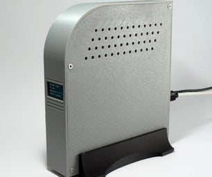
This time I have a single IC stereo amplifier which is based on TDA7377. This TDA7377 can be configured in different wattage modes as stated in the datasheet but for here we are using 1 channel for subwoofer and other one for speaker. The circuit is designed as per datasheet. The best thing is that this TDA IC can work with single 12volt power supply. And due to class AB operation need a very little heat sink. This is a demonstration tutorial to make amplifier using this IC, you can check the performance in the video also.
To keep the amplifier as small as possible, I am using PCB prototyping service offered by JLCPCB. JLCPCB is China based PCB manufacturer and dealing in PCB products like precision high layers, Stencils, 3d printing and SMT assembly. Get free coupons of worth $54 on 1st registration to JLCPCB using this link.
Attachments
Supplies
- TDA7377 Amplifier IC
- 10k resistor
- 100nF capacitor
- 47uf electrolytic capacitor
- Custom PCB from JLCPCB
Step 1: TDA7377 Details:
You can choose between different packages and get more details directly from official datasheet.
2 x 35W max./4Ω
2 x30W/4Ω EIAJ
2 x30W/4Ω EIAJ
2 x 20W/4Ω @14.4V, 1KHz, 10%
4 x 6W/4Ω @14.4V,1KHz, 10%
4 x 10W/2Ω @14.4V, 1KHz, 10%
Either we can use this IC in bridge mode or in simple mode. Because it has 4 channel max output which can give 6w per channel on a 4ohm load. And I am using the stereo + bridge configuration. Which makes a 2.1 channel amplifier (1 channel for subwoofer and two for speakers). The standby is kept on high for the amplifying action of the TDA7377. And we can build this 2.1 amplifier using minimal components.
Step 2: Circuit Diagram:
I made the circuit diagram in EasyEDA using the same schematics and from here we can convert the EDA file into PCB. Standby is pulled up for amplification and it can be used as a switch here, when connected to ground the amplifier remains silent (Stand-by mode).
Attachments
Step 3: PCB and Gerber Files:
Then I converted the schematics into GERBER files, you can download the same files from here. A very minimized PCB can be used because of minimal external components. We use input/ output coupling capacitors and power filtering capacitor for better performance. All the component values are mentioned in the PCB file.
These Gerber files can be used to order the PCB directly from JLCPCB, just upload them on website, choose the parameters- material, colour, thickness and finishing type. JLCPCB offers 5pcs of 2-layer PCB in just $2. Order them now from here and get discount coupons.
Wiring of amplifier is quite easy, we need 3 inputs to run this amplifier, either you can use a preamp or direct 3 channel input can be given. Headers mounting holes are given for the power input, audio input and output. Subwoofer connections and subwoofer input, speakers output and input are mentioned on the PCB silkscreen.
Step 4: Assembly and Heatsink:
Because of 35watt mini package the IC already has a good copper heat dissipating sink, but it is recommended to add a 20x20mm heatsink with this IC. So that no thermal damage will be there. Soldering can be done very easily first by placing small resistor then capacitors and then TDA7377.
Step 5: Testing and Working:
Here is the testing video of this amplifier, I am using this with constant 12v power supply, it demands a maximum current of 2Amperes. So it is recommended to pair the amplifier with at least 2A power source. The performance is quite good you can use this 2.1 amp as a car stereo player, it is loud enough for a single room home theatre system.


