US9698455B2 - Multi-mode filter having at least one feed line and a phase array of coupling elements - Google Patents

Multi-mode filter having at least one feed line and a phase array of coupling elements Download PDF

Info

Publication number
US9698455B2
US9698455B2 US13/531,003 US201213531003A US9698455B2 US 9698455 B2 US9698455 B2 US 9698455B2 US 201213531003 A US201213531003 A US 201213531003A US 9698455 B2 US9698455 B2 US 9698455B2
Authority
US
United States
Prior art keywords
coupling
feed line
cavity filter
mode cavity
filter according
Prior art date
Legal status (The legal status is an assumption and is not a legal conclusion. Google has not performed a legal analysis and makes no representation as to the accuracy of the status listed.)
Expired - Fee Related, expires
Application number
US13/531,003
Other versions
US20130049896A1 (en
Inventor
David Robert HENDRY
Steven John Cooper
Peter Blakeborough Kenington
Current Assignee (The listed assignees may be inaccurate. Google has not performed a legal analysis and makes no representation or warranty as to the accuracy of the list.)
Mesaplexx Pty Ltd
Original Assignee
Mesaplexx Pty Ltd
Priority date (The priority date is an assumption and is not a legal conclusion. Google has not performed a legal analysis and makes no representation as to the accuracy of the date listed.)
Filing date
Publication date
Priority claimed from AU2011903389A external-priority patent/AU2011903389A0/en
Application filed by Mesaplexx Pty Ltd filed Critical Mesaplexx Pty Ltd
Priority to US13/531,003 priority Critical patent/US9698455B2/en
Assigned to MESAPLEXX PTY LTD reassignment MESAPLEXX PTY LTD ASSIGNMENT OF ASSIGNORS INTEREST (SEE DOCUMENT FOR DETAILS). Assignors: COOPER, STEVEN JOHN, HENDRY, David Robert, KENINGTON, PETER BLAKEBOROUGH
Publication of US20130049896A1 publication Critical patent/US20130049896A1/en
Application granted granted Critical
Publication of US9698455B2 publication Critical patent/US9698455B2/en
Expired - Fee Related legal-status Critical Current
Adjusted expiration legal-status Critical

Links

Images

Classifications

    • HELECTRICITY
    • H01ELECTRIC ELEMENTS
    • H01PWAVEGUIDES; RESONATORS, LINES, OR OTHER DEVICES OF THE WAVEGUIDE TYPE
    • H01P1/00Auxiliary devices
    • H01P1/20Frequency-selective devices, e.g. filters
    • H01P1/207Hollow waveguide filters
    • H01P1/208Cascaded cavities; Cascaded resonators inside a hollow waveguide structure
    • H01P1/2084Cascaded cavities; Cascaded resonators inside a hollow waveguide structure with dielectric resonators
    • H01P1/2086Cascaded cavities; Cascaded resonators inside a hollow waveguide structure with dielectric resonators multimode
    • HELECTRICITY
    • H01ELECTRIC ELEMENTS
    • H01PWAVEGUIDES; RESONATORS, LINES, OR OTHER DEVICES OF THE WAVEGUIDE TYPE
    • H01P1/00Auxiliary devices
    • H01P1/20Frequency-selective devices, e.g. filters
    • H01P1/207Hollow waveguide filters
    • H01P1/208Cascaded cavities; Cascaded resonators inside a hollow waveguide structure
    • H01P1/2088Integrated in a substrate
    • HELECTRICITY
    • H01ELECTRIC ELEMENTS
    • H01PWAVEGUIDES; RESONATORS, LINES, OR OTHER DEVICES OF THE WAVEGUIDE TYPE
    • H01P7/00Resonators of the waveguide type
    • H01P7/10Dielectric resonators
    • H01P7/105Multimode resonators
    • HELECTRICITY
    • H01ELECTRIC ELEMENTS
    • H01PWAVEGUIDES; RESONATORS, LINES, OR OTHER DEVICES OF THE WAVEGUIDE TYPE
    • H01P1/00Auxiliary devices
    • H01P1/20Frequency-selective devices, e.g. filters
    • H01P1/2002Dielectric waveguide filters
    • YGENERAL TAGGING OF NEW TECHNOLOGICAL DEVELOPMENTS; GENERAL TAGGING OF CROSS-SECTIONAL TECHNOLOGIES SPANNING OVER SEVERAL SECTIONS OF THE IPC; TECHNICAL SUBJECTS COVERED BY FORMER USPC CROSS-REFERENCE ART COLLECTIONS [XRACs] AND DIGESTS
    • Y10TECHNICAL SUBJECTS COVERED BY FORMER USPC
    • Y10TTECHNICAL SUBJECTS COVERED BY FORMER US CLASSIFICATION
    • Y10T29/00Metal working
    • Y10T29/49Method of mechanical manufacture
    • Y10T29/49002Electrical device making
    • Y10T29/49016Antenna or wave energy "plumbing" making

Definitions

  • the present invention relates to filters, and in particular to a multi-mode filter including a resonator body for use, for example, in frequency division duplexers for telecommunication applications.
  • All physical filters essentially consist of a number of energy storing resonant structures, with paths for energy to flow between the various resonators and between the resonators and the input/output ports.
  • the physical implementation of the resonators and the manner of their interconnections will vary from type to type, but the same basic concept applies to all.
  • Such a filter can be described mathematically in terms of a network of resonators coupled together, although the mathematical topology does not have to match the topology of the real filter.
  • Dielectric resonators have high-Q (low loss) characteristics which enable highly selective filters having a reduced size compared to cavity filters.
  • These single-mode filters tend to be built as a cascade of separated physical dielectric resonators, with various couplings therebetween and to the ports. These resonators are easily identified as distinct physical objects, and the couplings tend also to be easily identified.
  • Single-mode filters of this type may include a network of discrete resonators formed from ceramic materials in a “puck” shape, where each resonator has a single dominant resonance frequency, or mode. These resonators are often coupled together by providing openings between cavities in which the resonators are located. Typically, the resonators provide transmission poles or “zeros”, which can be tuned at particular frequencies to provide a desired filter response. A number of resonators will usually be required to achieve suitable filtering characteristics for commercial applications, resulting in filtering equipment of a relatively large size.
  • filters formed from dielectric resonators are in frequency division duplexers for microwave telecommunication applications.
  • Duplexers have traditionally been provided at base stations at the bottom of antenna supporting towers, although a current trend for microwave telecommunication system design is to locate filtering and signal processing equipment at the top of the tower to thereby minimise cabling lengths and thus reduce signal losses.
  • the size of single mode filters as described above can make these filters undesirable for implementation at the top of antenna towers.
  • Multi-mode filters implement several resonators in a single physical body, such that reductions in filter size can be obtained.
  • a silvered dielectric body can resonate in many different modes. Each of these modes can act as one of the resonators in a filter.
  • multi-mode filters The usual manner in which these multi-mode filters are implemented is to selectively couple the energy from an input port to a first one of the modes. The energy stored in the first mode is then coupled to different modes within the resonator by introducing specific defects into the shape of the body.
  • a multi-mode filter can be implemented as an effective cascade of resonators, in a similar way to conventional single mode filter implementations. Again, this technique results in transmission poles which can be tuned to provide a desired filter response.
  • Two or more triple-mode filters may still need to be cascaded together to provide a filter assembly with suitable filtering characteristics.
  • this cascade of filters may be achieved using a waveguide or aperture for providing coupling between two resonator mono-bodies.
  • Another approach includes using a single-mode combine resonator coupled between two dielectric mono-bodies to form a hybrid filter assembly as described in U.S. Pat. No. 6,954,122. In any case the physical complexity and hence manufacturing costs are even further increased.
  • a multi-mode cavity filter comprises a dielectric resonator body incorporating a piece of dielectric material, the piece of dielectric material having a shape such that the dielectric resonator body can support at least two substantially degenerate resonant modes; and a phased array of coupling elements for coupling signals to the piece of dielectric material.
  • the multi-mode cavity filter may further comprise a signal transmission line for transmitting a signal to at least one of the plurality of the coupling elements.
  • the phase of the signal at a particular coupling element along the transmission line may be determined by the position of that coupling element along the transmission line.
  • the transmission line may include at least one meander to increase the length of the transmission line.
  • the or each coupling element may be positioned at a predetermined distance along the transmission line such that the signal reaching the or each coupling element has a predetermined phase.
  • At least some of the plurality of coupling elements may be connected to each other in series.
  • the phased array of coupling elements may comprise a primary transmission line configured to feed signals to plurality of secondary transmission lines branching off the primary transmission line, wherein each of the plurality of secondary transmission lines is configured to transmit a signal to at least one coupling element.
  • the coupling elements may be electrically independent or isolated from one another.
  • the multi-mode cavity filter may further comprise an amplitude determination mechanism for determining the amplitude of a signal transmitted along the transmission line.
  • the relative amplitudes of signals transmitted to each of the coupling elements may be predetermined.
  • the plurality of coupling elements may be arranged in a substantially symmetrical array.
  • Some of the plurality of coupling elements may be input elements arranged to deliver signals to the piece of dielectric material, and others of the plurality of coupling elements may be output elements arranged to recover signals from the piece of dielectric material. At least one input element may be coupled to at least one output element.
  • the piece of dielectric material may comprise at least two faces, the input elements may be arranged on a first of the at least two faces, and the output elements may be arranged on a second of the at least two faces.
  • the input and output elements may be arranged on a single face.
  • At least some of the plurality of coupling elements may be patches formed on a surface of the piece of dielectric material. At least some of the patches may be of a regular geometric shape. Additionally or alternatively, at least some of the patches may be of an irregular geometric shape.
  • At least some of the plurality of coupling elements may be probes arranged to abut a surface of, or at least partially penetrate a surface of, the piece of dielectric material.
  • the probes may have a substantially circular cross section.
  • a shielding element may be associated with each probe.
  • At least some of the plurality of coupling elements may be magnetic field generating elements.
  • the magnetic field generating elements may be loop elements.
  • the plurality of coupling elements may comprise at least a first set of coupling elements configured to couple a first signal to the piece of dielectric material for exciting a first resonant mode of the dielectric resonator, and a second set of coupling elements configured to couple a second signal to the piece of dielectric material for exciting a second resonant mode of the dielectric resonator.
  • a method of manufacturing a multi-mode cavity filter comprises: providing a resonator body of dielectric material capable of supporting at least two substantially degenerate resonant modes; and providing a phased array of coupling elements for coupling signals to the piece of dielectric material.
  • a multi-mode cavity filter may comprise a dielectric resonator body incorporating a piece of dielectric material, the piece of dielectric material having a shape such that the dielectric resonator body can support at least two substantially degenerate resonant modes; and a coupling structure comprising a plurality of independent coupling elements for coupling signals to the piece of dielectric material.
  • At least some of the plurality of coupling elements may be connected to each other in series.
  • the multi-mode cavity filter may further comprise a primary transmission line configured to transmit signals to a plurality of secondary transmission lines branching off the primary transmission line, wherein each of the plurality of secondary transmission lines is configured to feed a signal to a single coupling element.
  • a method of manufacturing a multi-mode cavity filter may comprise: providing a resonator body of dielectric material capable of supporting at least two substantially degenerate resonant modes, and providing a coupling structure comprising a plurality of coupling elements for coupling signals to the piece of dielectric material.
  • FIG. 1 is a schematic perspective view of an example of a multi-mode filter
  • FIG. 2 is a schematic underside view of the multi-mode filter of FIG. 1 ;
  • FIG. 3 is a schematic side view of a further example of a multi-mode filter
  • FIG. 4 is a schematic underside view of the multi-mode filter of FIG. 3 ;
  • FIG. 5 is a schematic side view of a further example of the multi-mode filter of FIG. 3 ;
  • FIG. 6 is a schematic side view of a further example of the multi-mode filter of FIG. 5 ;
  • FIG. 7 is a schematic underside view of a further example of a multi-mode filter.
  • FIGS. 8 to 11 are schematic underside views of further examples of the multi-mode filter of FIG. 7 .
  • FIG. 1 shows a filter 100 having a resonator body 102 which is coupled by a coupling structure 104 (not shown in FIG. 1 , but shown in FIGS. 2 to 4, and 7 to 11 ) to a substrate 106 .
  • the coupling structure 104 is located on a surface of the resonator body 102 that is adjacent to the substrate 106 .
  • the substrate 106 and the coupling structure 104 will be discussed in further detail below.
  • the resonator body 102 is formed from a piece of dielectric material having suitable dielectric properties.
  • the resonator body 102 is a ceramic material, although this is not essential and alternative materials can be used.
  • the body 102 can be a multilayered body including, for example, layers of materials having different dielectric properties.
  • the body 102 can include a core of a dielectric material, and one or more outer layers of different dielectric materials.
  • the coupling structure 104 provides coupling to a plurality of the resonance modes of the resonator body.
  • a radio frequency signal containing, say, frequencies from within the 1 MHz to 100 GHz range, can be supplied to or received from the coupling structure 104 .
  • this allows a signal to be filtered to be supplied to the resonator body 102 for filtering, or can allow a filtered signal to be obtained from the resonator body, as will be described in more detail below.
  • an electrically conductive coupling structure formed from an array of individual elements electrically independent from one another allows the signal to be coupled to a plurality of resonance modes of the resonator body 102 .
  • This allows a more simplified configuration of resonator body 102 and coupling structure 104 to be used as compared to traditional arrangements. For example, this avoids the need to have a resonator body including cut-outs or other complicated shapes, as well as avoiding the need for coupling structures that extend into the resonator body. This, in turn, makes the filter less expensive and simpler to manufacture, and can provide enhanced filtering characteristics.
  • the filter is small in size, typically of the order of 6000 mm 3 per resonator body, making the filter apparatus suitable for use at the top of antenna towers. It will be appreciated by those skilled in the art that, while the individual coupling elements are electrically independent from one another, there will inevitably be some degree of mutual coupling between some couplings which will need to be taken into account in the design of the filter. This mutual coupling is, however, incidental, and not an intended part of the operation of the invention.
  • the resonator body 102 usually includes an external coating ( FIG. 2 ; 110 ) of conductive material, such as silver, although other materials could be used such as gold, copper, or the like.
  • the conductive material may be applied to one or more surfaces of the body.
  • a region of the surface adjacent the coupling structure 104 that is the surface at which the resonator body 102 is coupled to the substrate 106 , may be uncoated to allow coupling of signals to the resonator body.
  • the resonator body 102 can be any shape, but generally defines at least two orthogonal axes.
  • the resonator body 102 is a cuboid body, and therefore defines three orthogonal axes substantially aligned with surfaces of the resonator body, as shown by the axes X, Y, Z.
  • the resonator body 102 has three dominant resonance modes that are substantially orthogonal and substantially aligned with the three orthogonal axes.
  • Cuboid structures are particularly advantageous as they can be easily and inexpensively manufactured, and can also be easily fitted together, for example by arranging multiple resonator bodies in contact. Cuboid structures typically have clearly defined resonance modes, making configuration of the coupling structure more straightforward. Additionally, the use of a cuboid structure provides a planar surface so that the coupling structure can be arranged in a single plane parallel to the planar surface. This can help maximise coupling between the couplings and resonator body 102 , as well as allowing the coupling structure 104 to be more easily manufactured.
  • the couplings may be provided on the substrate 106 .
  • the provision of a planar surface 108 allows the substrate 106 to be a planar substrate, such as a printed circuit board (PCB) or the like.
  • PCB printed circuit board
  • alternative arrangements can be used, such as coating the coupling structure 104 onto the resonator body directly.
  • resonance modes of the resonator body provide respective energy paths between the input and output.
  • the input coupling and the output coupling can be configured to allow coupling therebetween to provide an energy path separate to energy paths provided by the resonance modes of the resonator body.
  • This can provide four parallel energy paths between the input and the output.
  • These energy paths can be arranged to introduce at least one transmission zero to the frequency response of the filter, as will be described in more detail below.
  • zero refers to a transmission minimum in the frequency response of the filter, meaning transmission of signals at that frequency will be minimal, as will be understood by persons skilled in the art.
  • the filter 100 includes a resonator body 102 ( FIG. 1 ) having a surface 108 ( FIG. 2 ) at which the body is coupled to the substrate 106 .
  • a coating 110 of conductive material (such as metal) is formed around the periphery of the surface 108 .
  • the coating 110 may be formed on at least one of the other faces of the resonator body 102 . In some embodiments, all of the other faces of the resonator body 102 are at least partially coated by the coating 110 .
  • the surface 108 of the body adjacent the substrate 106 is left substantially uncoated to allow signals to be coupled to the resonator body 102 , with the remainder of the surface, which is coated, being electrically connected to the groundplane located on, or within the substrate.
  • the coupling structure 104 of this embodiment is formed from an array of pads or patches 112 insulated from each other and through which signals are transmitted to and/or recovered from the resonator body 102 .
  • the mutual insulation of each patch keeps the interference of signals between the patches to a minimum.
  • the coupling structure 104 includes an array of sixteen substantially square patches 112 arranged in a 4 by 4 configuration.
  • the patches 112 are configured to couple to a track or to connectors on the substrate 106 .
  • the patches 112 may be connected to a printed circuit board (not shown) via which signals are fed to the resonator body 102 .
  • Each of the patches 112 includes at least one connection, or feed point (not shown), to which a feed line (not shown) can be connected for provision of a signal to the patch.
  • each patch 112 includes two or more feed points.
  • the or each feed point is located centrally within the patch 112 whereas, in other embodiments, the or each feed point is located offset from the centre of the patch.
  • each of the patches 112 has a square shape
  • the patches can be any shape.
  • the patches 112 are compact shapes such as circles, triangles, squares, pentagons and the like.
  • the patches 112 are elongated shapes such as rectangles, ellipses and the like.
  • all of the patches 112 are the same shape, in other embodiments, a combination of patches of different compact geometric shapes, or a combination of patches of compact and elongated geometric shapes may be used.
  • Patches 112 of compact geometric shapes have greater rotational symmetry than patches of elongated geometric shapes and, consequently, compact geometric shaped patches couple predominantly to the electric field (E-field), with relatively little coupling to the magnetic field (H-field). In contrast, patches having elongated geometric shapes couple to a greater degree to the H-field in addition to the E-field coupling.
  • the size of the patches is also determinative with regard to the strength with which the patches couple to the E-field and to the H-field. Relatively small patches couple primarily to the E-field. Relatively large patches contribute an amount of H-field coupling in addition to the E-field coupling. It will be appreciated that a combination of patches of different sizes may be used to achieve a desired coupling to the E-field and the H-field.
  • Another factor that determines the amount by which the patches 112 contribute to the E-field and the H-field is the position of the feed point (that is, the signal input point) into each patch. If the point at which a signal is fed into a patch 112 is substantially central in the patch, then the predominant excitation provided by the patch is an E-field excitation. However, if the signal is fed into the patch at a point offset from the centre, then H-field excitation is generated in addition to an E-field excitation.
  • FIGS. 3 and 4 show a side view and an underside view respectively of an alternative embodiment of the invention in which the coupling structure 104 is formed from an array of probes 114 .
  • Each of the probes 114 is an elongate conductor which is configured to couple, at one end, to a track or to connectors on the substrate 106 , and at the other end, to the surface 108 of the resonator body 102 ( FIG. 3 ).
  • the probes 114 are substantially circular in cross section (see FIG. 4 ).
  • probes having other cross sections, such as square or elliptical, may be used in alternative embodiments.
  • FIG. 3 A number of connections, such as a connection between the metallic coating 110 and a track or groundplane layer on the substrate 106 , have been omitted from FIG. 3 (and FIGS. 5 and 6 ) for clarity. Those skilled in the art will appreciate, however, that the filter 100 may include further connections and components not essential to the understanding of this invention and which have been omitted from the drawings.
  • the probes 114 may be arranged in a regular array, for example in a 4 by 4 configuration. Alternatively, a smaller or larger array may be used, and/or the probes may be arranged in an irregular configuration.
  • the resonator body 102 is shown having a coupling structure 104 which includes an array of probes 114 which penetrate the surface 108 of the resonator body 102 .
  • Each probe 114 is configured to fit into one of an array of complementary-shaped recesses 116 formed in the resonator body 102 .
  • the probes 114 penetrate a short depth into the resonator body 102 .
  • the probes 114 penetrate a substantial proportion of their length into the resonator body 102 . The lengths of the probes 114 has an effect on the degree of coupling afforded from the probe to the resonator body 102 .
  • the lengths of the probes can be chosen according to the coupling required at each probe 114 .
  • some probes 114 in an array can have lengths that differ from other probes in the array, thereby creating a desired field pattern to excite particular modes within the resonator body 102 .
  • FIG. 6 shows an alternative embodiment of the invention in which each of the probes 114 includes a shielding element 118 .
  • Each shielding element 118 is a grounded conductor which at least partially surrounds a corresponding probe 114 .
  • the shielding elements 118 are configured and positioned such that they are in contact with the metallic coating 110 surrounding the resonator body 102 , and may take any known form, such as a wire mesh ring or a solid shield. In some embodiments, where the probes 114 are shorter than a particular length, shielding elements 118 are not required and may, therefore, be omitted.
  • the degree of coupling of the signal from each probe 114 to a resonance mode of the resonator body 102 is, in part, determined by the length of the probe.
  • the length of each probe 114 also has an effect on the degree of H-field coupling relative to the E-field coupling from the probe. Additionally, the amount by which a probe 114 penetrates into the resonator body 102 affects the degree of coupling from the probe.
  • a relatively long probe which penetrates relatively deeply into the resonator body 102 generates a greater H-field coupling than a relatively shorter probe, or a probe that penetrates a shorter depth into the resonator body 102 .
  • a relatively very short probe 114 contributes little or no H-field coupling.
  • What constitutes ‘long’ and ‘short’ in terms of probe length depends on the degree of penetration of the probe into the resonator body 102 : a short probe is one which has minimal penetration into the body, and a long probe is one which penetrates the body to a significant degree.
  • the coupling structure 104 includes an array of loop elements (not shown), which may be arranged in a configuration similar to those described above.
  • the loop elements serve to couple substantially to the H-field, with relatively little E-field coupling occurring.
  • FIG. 7 shows an embodiment in which the coupling structure 104 includes two types of couplings: input couplings 104 a (shown with hatching), and output couplings 104 b (shown without hatching).
  • input couplings 104 a shown with hatching
  • output couplings 104 b shown without hatching
  • different coupling structures can be provided on different surfaces of the resonator body.
  • a further alternative is for a coupling structure to extend over multiple surfaces of the resonator body, with different coupling elements being provided on different surfaces (for example, an array of input couplings on one surface of the resonator body 102 and an array of output couplings on a different surface of the resonator body), or with coupling elements extending over multiple surfaces.
  • Such arrangements can be used to allow a particular configuration of input and output to be accommodated, for example to meet physical constraints associated with other equipment, or to allow alternative coupling arrangements to be provided.
  • a configuration of the input and output coupling elements, along with the configuration of the resonator body 102 controls a degree of coupling with each of the plurality of resonance modes and hence the properties of the filter, such as the frequency response.
  • one or more of the inputs are coupled to one or more of the outputs and vice versa.
  • Signals are fed to each of the patches 112 and probes 114 via one or more transmission or feed lines.
  • the feed lines may take the form, for example, of a track on a PCB.
  • a feed line 120 is connected to a plurality of input couplings 104 a in series.
  • the feed line 120 is coupled only to the input couplings 104 a .
  • the feed line may be coupled to more or fewer patches 112 or probes 114 .
  • the meandering nature of the feed line 120 allows a designer of the filter 100 to select which coupling elements the feed line is connected to, and the order in which they are connected.
  • the length of the feed line can be selected such that the signal arriving at any particular coupling element has a desired phase.
  • the input couplings 104 a receive signals via an alternative to a single feed line 120 ( FIG. 8 ).
  • a primary feed line 120 a transmits signals to a plurality of secondary feed lines 120 b which, in turn, transmit signals to the input couplings 104 a .
  • the structure of the primary and secondary feed lines in this example resemble a “star” or “spider” arrangement.
  • the impedance of the feed lines is another factor that affects the degree of coupling of the signal to the resonance modes in the resonator body 102 .
  • FIGS. 8 and 9 show alternative arrangements of feed or transmission lines 120 that transmit signals from a signal source (not shown) to one or more of the coupling elements of the coupling structure 104 .
  • the length of the feed line along which a signal is transmitted affects the phase of the signal when it arrives at a coupling element. That is to say, a first signal that travels comparatively greater distance along a feed line to a coupling element will be at least partially out of phase with a second signal that travels a comparatively shorter distance along a feed line.
  • the extra distance travelled by a first signal is equal to one complete cycle of the that signal, then the first and second signals would be in phase with one another.
  • the relative phases of signals at the coupling elements can be dictated by configuring the length of the feed line along which the signals are transmitted. By dictating the phase of the signals at each coupling element, it is possible to control higher-order spurious modes and, preferably, reduce their amplitude. By reducing the amplitude of the spurious higher-order modes, filter designers are able to meet demanding filter specifications without the need to make significant, complex and expensive structural modifications to the dielectric material or the need to provide additional filtering stages to attenuate the unwanted responses.
  • FIG. 10 shows an underside view of the resonator body 102 with a plurality of input couplings 104 a and a plurality of output couplings 104 b .
  • a feed line 122 provides a connection between all of the input couplings 104 a .
  • the feed line 122 of FIG. 10 includes a number of junctions 122 a which allow the feed line to be directed to desired coupling elements on the resonator body 102 .
  • the feed line 122 includes a number of meanders 122 b which serve to increase the length of the feed line between coupling elements on the line.
  • the distance that a signal travels along a feed line dictates, in part, the phase of the signal at a coupling element. Therefore, it is possible to achieve a phase of a signal at a particular coupling element by designing the feed line such that the signal travels an appropriate distance along the feed line to reach the coupling element.
  • the feed line is shown to meander in this invention, other mechanisms for increasing the length of the feed line could alternatively be used.
  • the feed line may comprise a single continuous feed line with no junctions, and incorporating fewer or more meanders or similar mechanisms for increasing the length of the feed line between coupling elements.
  • the feed line arrangement may be similar to the arrangement shown in FIG.
  • a primary feed line 124 a transmits signals to a plurality of secondary feed lines 124 b , each of which is coupled to a coupling element. While, in this example, only five secondary feed lines 124 b are shown, in practice, any number of secondary feed lines may be incorporated, connecting the primary feed line 124 a to any number of coupling elements, as required by the design of the filter.
  • the length of the feed line 122 feeding each coupling element is calculated, based on the desired phase at each coupling element, using an electromagnetic simulation tool, such as CST Microwave Studio, manufactured by Computer Simulation Technology AG.
  • a concept known as amplitude tapering may be used to control and specify the amplitude across the array of coupling elements.
  • the amplitude of the signal transmitted to coupling elements at the centre of the array is greater than the amplitude of the signal or signals transmitted to coupling elements surrounding the central element, and the coupling elements around the periphery of the array.
  • This concept is advantageous in targeting the excitation predominantly to a specific mode, for example, in the case of an array of patches, this mechanism would target a known mode such as the TM110 mode.
  • the amplitude of the signal transmitted to coupling elements at the centre of the array is lower than the amplitude of the signal or signals transmitted to coupling elements surrounding the central element, and the coupling elements around the periphery of the array.
  • An advantage of the above-described examples is that, by controlling particular design aspects of the filter, such as the size, shape and location of the coupling elements, and the length and other aspects of the transmission line feeding signals to the coupling elements, it is possible to accurately control the fields generated as a result of the signal and, thus, the excitation modes of the resonator body that are excited by the signals.
  • a cuboid resonator body 102 is used. Such a resonator body enables coupling of up to three resonance modes. However, as will be apparent to those skilled in the art, a resonator body of a different three-dimensional shape may provide a different number of degenerate resonance modes. For example, a rectangular cuboid resonator body (that is a 2:2:1 ratio cuboid) has four degenerate resonance modes.
  • filters can be designed having one or more resonator bodies or the same or different shapes, depending on the required characteristics of the filter.
  • characteristics of a filter may be chosen by applying defects to the resonator body. Such defects may include shaving a particular amount of dielectric material from an edge of the resonator body, or drilling one or more holes of a particular size into the body.
  • a single resonator body cannot provide adequate performance (for example, attenuation of out of band signals).
  • filter performance can be improved by providing two or more resonator bodies arranged in series, to thereby implement a higher-performance filter.
  • this can be achieved by providing two resonator bodies in contact with each other, with one or more apertures provided in the silver coatings of the resonator bodies, where the bodies are in contact. This allows the fields in each cube to enter the adjacent cube, so that a resonator body can receive a signal from or provide a signal to another resonator body.
  • this allows each resonator body to include only a single coupling array, with a coupling array on one resonator body acting as an input and the coupling array on the other resonator body acting as an output.
  • the input of a downstream filter can be coupled to the output of an upstream filter using a suitable connection such as a short transmission line.

Abstract

A multi-mode cavity filter includes a dielectric resonator body incorporating a piece of dielectric material, the piece of dielectric material having a shape such that it can support at least two substantially degenerate resonant modes; and a phased array of coupling elements for coupling signals to the piece of dielectric material.

Description

CROSS REFERENCE TO RELATED APPLICATIONS
The present application is related to and claims the benefit of Australian Provisional Patent Application No. 2011903389, filed Aug. 23, 2011 and U.S. Provisional Patent Application No. 61/531,277, filed Sep. 6, 2011, both of whose disclosures are hereby incorporated by reference in their entirety into the present disclosure.
TECHNICAL FIELD
The present invention relates to filters, and in particular to a multi-mode filter including a resonator body for use, for example, in frequency division duplexers for telecommunication applications.
BACKGROUND
The reference in this specification to any prior publication (or information derived therefrom), or to any matter which is known, is not, and should not be taken as an acknowledgment or admission or any form of suggestion that the prior publication (or information derived therefrom) or known matter forms part of the common general knowledge in the field of endeavour to which this specification relates.
All physical filters essentially consist of a number of energy storing resonant structures, with paths for energy to flow between the various resonators and between the resonators and the input/output ports. The physical implementation of the resonators and the manner of their interconnections will vary from type to type, but the same basic concept applies to all. Such a filter can be described mathematically in terms of a network of resonators coupled together, although the mathematical topology does not have to match the topology of the real filter.
Conventional single-mode filters formed from dielectric resonators are known. Dielectric resonators have high-Q (low loss) characteristics which enable highly selective filters having a reduced size compared to cavity filters. These single-mode filters tend to be built as a cascade of separated physical dielectric resonators, with various couplings therebetween and to the ports. These resonators are easily identified as distinct physical objects, and the couplings tend also to be easily identified.
Single-mode filters of this type may include a network of discrete resonators formed from ceramic materials in a “puck” shape, where each resonator has a single dominant resonance frequency, or mode. These resonators are often coupled together by providing openings between cavities in which the resonators are located. Typically, the resonators provide transmission poles or “zeros”, which can be tuned at particular frequencies to provide a desired filter response. A number of resonators will usually be required to achieve suitable filtering characteristics for commercial applications, resulting in filtering equipment of a relatively large size.
One example application of filters formed from dielectric resonators is in frequency division duplexers for microwave telecommunication applications. Duplexers have traditionally been provided at base stations at the bottom of antenna supporting towers, although a current trend for microwave telecommunication system design is to locate filtering and signal processing equipment at the top of the tower to thereby minimise cabling lengths and thus reduce signal losses. However, the size of single mode filters as described above can make these filters undesirable for implementation at the top of antenna towers.
Multi-mode filters implement several resonators in a single physical body, such that reductions in filter size can be obtained. As an example, a silvered dielectric body can resonate in many different modes. Each of these modes can act as one of the resonators in a filter. In order to provide a practical multi-mode filter it is necessary to couple the energy between the modes within the body, in contrast with the coupling between discrete objects in single mode filters, which coupling is easier to control in practice.
The usual manner in which these multi-mode filters are implemented is to selectively couple the energy from an input port to a first one of the modes. The energy stored in the first mode is then coupled to different modes within the resonator by introducing specific defects into the shape of the body. In this manner, a multi-mode filter can be implemented as an effective cascade of resonators, in a similar way to conventional single mode filter implementations. Again, this technique results in transmission poles which can be tuned to provide a desired filter response.
An example of such an approach is described in U.S. Pat. No. 6,853,271, which is directed towards a triple-mode mono-body filter. Energy is coupled into a first mode of a dielectric-filled mono-body resonator, using a suitably configured input probe provided in a hole formed on a face of the resonator. The coupling between this first mode and two other modes of the resonator is accomplished by selectively providing corner cuts or slots on the resonator body.
This technique allows for substantial reductions in filter size because a triple-mode filter of this type represents the equivalent of a single-mode filter composed of three discrete single mode resonators. However, the approach used to couple energy into and out of the resonator, and between the modes within the resonator to provide the effective resonator cascade, requires the body to be of complicated shape, increasing manufacturing costs.
Two or more triple-mode filters may still need to be cascaded together to provide a filter assembly with suitable filtering characteristics. As described in U.S. Pat. Nos. 6,853,271 and 7,042,314, this cascade of filters may be achieved using a waveguide or aperture for providing coupling between two resonator mono-bodies. Another approach includes using a single-mode combine resonator coupled between two dielectric mono-bodies to form a hybrid filter assembly as described in U.S. Pat. No. 6,954,122. In any case the physical complexity and hence manufacturing costs are even further increased.
SUMMARY OF THE INVENTION
According to a first aspect, a multi-mode cavity filter comprises a dielectric resonator body incorporating a piece of dielectric material, the piece of dielectric material having a shape such that the dielectric resonator body can support at least two substantially degenerate resonant modes; and a phased array of coupling elements for coupling signals to the piece of dielectric material.
The multi-mode cavity filter may further comprise a signal transmission line for transmitting a signal to at least one of the plurality of the coupling elements. The phase of the signal at a particular coupling element along the transmission line may be determined by the position of that coupling element along the transmission line.
The transmission line may include at least one meander to increase the length of the transmission line.
The or each coupling element may be positioned at a predetermined distance along the transmission line such that the signal reaching the or each coupling element has a predetermined phase.
At least some of the plurality of coupling elements may be connected to each other in series.
The phased array of coupling elements may comprise a primary transmission line configured to feed signals to plurality of secondary transmission lines branching off the primary transmission line, wherein each of the plurality of secondary transmission lines is configured to transmit a signal to at least one coupling element.
The coupling elements may be electrically independent or isolated from one another.
The multi-mode cavity filter may further comprise an amplitude determination mechanism for determining the amplitude of a signal transmitted along the transmission line. The relative amplitudes of signals transmitted to each of the coupling elements may be predetermined.
The plurality of coupling elements may be arranged in a substantially symmetrical array.
Some of the plurality of coupling elements may be input elements arranged to deliver signals to the piece of dielectric material, and others of the plurality of coupling elements may be output elements arranged to recover signals from the piece of dielectric material. At least one input element may be coupled to at least one output element.
The piece of dielectric material may comprise at least two faces, the input elements may be arranged on a first of the at least two faces, and the output elements may be arranged on a second of the at least two faces. Alternatively, the input and output elements may be arranged on a single face.
At least some of the plurality of coupling elements may be patches formed on a surface of the piece of dielectric material. At least some of the patches may be of a regular geometric shape. Additionally or alternatively, at least some of the patches may be of an irregular geometric shape.
At least some of the plurality of coupling elements may be probes arranged to abut a surface of, or at least partially penetrate a surface of, the piece of dielectric material. The probes may have a substantially circular cross section.
A shielding element may be associated with each probe.
At least some of the plurality of coupling elements may be magnetic field generating elements. The magnetic field generating elements may be loop elements.
The plurality of coupling elements may comprise at least a first set of coupling elements configured to couple a first signal to the piece of dielectric material for exciting a first resonant mode of the dielectric resonator, and a second set of coupling elements configured to couple a second signal to the piece of dielectric material for exciting a second resonant mode of the dielectric resonator.
According to a second aspect, a method of manufacturing a multi-mode cavity filter comprises: providing a resonator body of dielectric material capable of supporting at least two substantially degenerate resonant modes; and providing a phased array of coupling elements for coupling signals to the piece of dielectric material.
According to another embodiment, a multi-mode cavity filter may comprise a dielectric resonator body incorporating a piece of dielectric material, the piece of dielectric material having a shape such that the dielectric resonator body can support at least two substantially degenerate resonant modes; and a coupling structure comprising a plurality of independent coupling elements for coupling signals to the piece of dielectric material.
At least some of the plurality of coupling elements may be connected to each other in series.
The multi-mode cavity filter may further comprise a primary transmission line configured to transmit signals to a plurality of secondary transmission lines branching off the primary transmission line, wherein each of the plurality of secondary transmission lines is configured to feed a signal to a single coupling element.
According to another embodiment, a method of manufacturing a multi-mode cavity filter may comprise: providing a resonator body of dielectric material capable of supporting at least two substantially degenerate resonant modes, and providing a coupling structure comprising a plurality of coupling elements for coupling signals to the piece of dielectric material.
BRIEF DESCRIPTION OF THE DRAWINGS
For a better understanding of the present invention, and to show more clearly how the invention may be carried into effect, reference will now be made, by way of example, to the following drawings, in which:
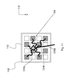
FIG. 1 is a schematic perspective view of an example of a multi-mode filter;
FIG. 2 is a schematic underside view of the multi-mode filter of FIG. 1;
FIG. 3 is a schematic side view of a further example of a multi-mode filter;
FIG. 4 is a schematic underside view of the multi-mode filter of FIG. 3;
FIG. 5 is a schematic side view of a further example of the multi-mode filter of FIG. 3;
FIG. 6 is a schematic side view of a further example of the multi-mode filter of FIG. 5;
FIG. 7 is a schematic underside view of a further example of a multi-mode filter; and
FIGS. 8 to 11 are schematic underside views of further examples of the multi-mode filter of FIG. 7.
DETAILED DESCRIPTION OF THE INVENTION
An example of a multi-mode filter will now be described with reference to the drawings, where like features in different drawings are denoted by the same reference numbers.
FIG. 1 shows a filter 100 having a resonator body 102 which is coupled by a coupling structure 104 (not shown in FIG. 1, but shown in FIGS. 2 to 4, and 7 to 11) to a substrate 106. The coupling structure 104 is located on a surface of the resonator body 102 that is adjacent to the substrate 106. The substrate 106 and the coupling structure 104 will be discussed in further detail below. The resonator body 102 is formed from a piece of dielectric material having suitable dielectric properties. In one example, the resonator body 102 is a ceramic material, although this is not essential and alternative materials can be used. Additionally, the body 102 can be a multilayered body including, for example, layers of materials having different dielectric properties. In one example, the body 102 can include a core of a dielectric material, and one or more outer layers of different dielectric materials.
The coupling structure 104 provides coupling to a plurality of the resonance modes of the resonator body. In use, a radio frequency signal, containing, say, frequencies from within the 1 MHz to 100 GHz range, can be supplied to or received from the coupling structure 104. In a suitable configuration, this allows a signal to be filtered to be supplied to the resonator body 102 for filtering, or can allow a filtered signal to be obtained from the resonator body, as will be described in more detail below.
The use of an electrically conductive coupling structure formed from an array of individual elements electrically independent from one another allows the signal to be coupled to a plurality of resonance modes of the resonator body 102. This allows a more simplified configuration of resonator body 102 and coupling structure 104 to be used as compared to traditional arrangements. For example, this avoids the need to have a resonator body including cut-outs or other complicated shapes, as well as avoiding the need for coupling structures that extend into the resonator body. This, in turn, makes the filter less expensive and simpler to manufacture, and can provide enhanced filtering characteristics. In addition, the filter is small in size, typically of the order of 6000 mm3 per resonator body, making the filter apparatus suitable for use at the top of antenna towers. It will be appreciated by those skilled in the art that, while the individual coupling elements are electrically independent from one another, there will inevitably be some degree of mutual coupling between some couplings which will need to be taken into account in the design of the filter. This mutual coupling is, however, incidental, and not an intended part of the operation of the invention.
A number of further features will now be described.
The resonator body 102 usually includes an external coating (FIG. 2; 110) of conductive material, such as silver, although other materials could be used such as gold, copper, or the like. The conductive material may be applied to one or more surfaces of the body. A region of the surface adjacent the coupling structure 104, that is the surface at which the resonator body 102 is coupled to the substrate 106, may be uncoated to allow coupling of signals to the resonator body.
The resonator body 102 can be any shape, but generally defines at least two orthogonal axes. In the current example, the resonator body 102 is a cuboid body, and therefore defines three orthogonal axes substantially aligned with surfaces of the resonator body, as shown by the axes X, Y, Z. As a result, the resonator body 102 has three dominant resonance modes that are substantially orthogonal and substantially aligned with the three orthogonal axes.
Cuboid structures are particularly advantageous as they can be easily and inexpensively manufactured, and can also be easily fitted together, for example by arranging multiple resonator bodies in contact. Cuboid structures typically have clearly defined resonance modes, making configuration of the coupling structure more straightforward. Additionally, the use of a cuboid structure provides a planar surface so that the coupling structure can be arranged in a single plane parallel to the planar surface. This can help maximise coupling between the couplings and resonator body 102, as well as allowing the coupling structure 104 to be more easily manufactured.
For example, the couplings may be provided on the substrate 106. In this instance, the provision of a planar surface 108 (FIG. 2) allows the substrate 106 to be a planar substrate, such as a printed circuit board (PCB) or the like. However, alternative arrangements can be used, such as coating the coupling structure 104 onto the resonator body directly.
In use, resonance modes of the resonator body provide respective energy paths between the input and output. Furthermore, the input coupling and the output coupling can be configured to allow coupling therebetween to provide an energy path separate to energy paths provided by the resonance modes of the resonator body. This can provide four parallel energy paths between the input and the output. These energy paths can be arranged to introduce at least one transmission zero to the frequency response of the filter, as will be described in more detail below. In this regard, the term “zero” refers to a transmission minimum in the frequency response of the filter, meaning transmission of signals at that frequency will be minimal, as will be understood by persons skilled in the art.
A specific example filter is shown in FIG. 2. In this example, the filter 100 includes a resonator body 102 (FIG. 1) having a surface 108 (FIG. 2) at which the body is coupled to the substrate 106. A coating 110 of conductive material (such as metal) is formed around the periphery of the surface 108. The coating 110 may be formed on at least one of the other faces of the resonator body 102. In some embodiments, all of the other faces of the resonator body 102 are at least partially coated by the coating 110. However, as noted above, the surface 108 of the body adjacent the substrate 106 is left substantially uncoated to allow signals to be coupled to the resonator body 102, with the remainder of the surface, which is coated, being electrically connected to the groundplane located on, or within the substrate.
The coupling structure 104 of this embodiment is formed from an array of pads or patches 112 insulated from each other and through which signals are transmitted to and/or recovered from the resonator body 102. The mutual insulation of each patch keeps the interference of signals between the patches to a minimum. In the embodiment shown in FIG. 2, the coupling structure 104 includes an array of sixteen substantially square patches 112 arranged in a 4 by 4 configuration. The patches 112 are configured to couple to a track or to connectors on the substrate 106. As an alternative to being connected directly to the substrate 106, in other embodiments, the patches 112 may be connected to a printed circuit board (not shown) via which signals are fed to the resonator body 102.
Each of the patches 112 includes at least one connection, or feed point (not shown), to which a feed line (not shown) can be connected for provision of a signal to the patch. In some embodiments, each patch 112 includes two or more feed points. Similarly, in some embodiments, the or each feed point is located centrally within the patch 112 whereas, in other embodiments, the or each feed point is located offset from the centre of the patch.
Although, in this embodiment, each of the patches 112 has a square shape, the patches can be any shape. In some embodiments, the patches 112 are compact shapes such as circles, triangles, squares, pentagons and the like. In other embodiments, the patches 112 are elongated shapes such as rectangles, ellipses and the like. Similarly, while, in this embodiment, all of the patches 112 are the same shape, in other embodiments, a combination of patches of different compact geometric shapes, or a combination of patches of compact and elongated geometric shapes may be used. Patches 112 of compact geometric shapes have greater rotational symmetry than patches of elongated geometric shapes and, consequently, compact geometric shaped patches couple predominantly to the electric field (E-field), with relatively little coupling to the magnetic field (H-field). In contrast, patches having elongated geometric shapes couple to a greater degree to the H-field in addition to the E-field coupling.
In addition to the shape of the patches 112, the size of the patches is also determinative with regard to the strength with which the patches couple to the E-field and to the H-field. Relatively small patches couple primarily to the E-field. Relatively large patches contribute an amount of H-field coupling in addition to the E-field coupling. It will be appreciated that a combination of patches of different sizes may be used to achieve a desired coupling to the E-field and the H-field.
Another factor that determines the amount by which the patches 112 contribute to the E-field and the H-field is the position of the feed point (that is, the signal input point) into each patch. If the point at which a signal is fed into a patch 112 is substantially central in the patch, then the predominant excitation provided by the patch is an E-field excitation. However, if the signal is fed into the patch at a point offset from the centre, then H-field excitation is generated in addition to an E-field excitation.
FIGS. 3 and 4 show a side view and an underside view respectively of an alternative embodiment of the invention in which the coupling structure 104 is formed from an array of probes 114. Each of the probes 114 is an elongate conductor which is configured to couple, at one end, to a track or to connectors on the substrate 106, and at the other end, to the surface 108 of the resonator body 102 (FIG. 3). In this embodiment, the probes 114 are substantially circular in cross section (see FIG. 4). However, probes having other cross sections, such as square or elliptical, may be used in alternative embodiments. A number of connections, such as a connection between the metallic coating 110 and a track or groundplane layer on the substrate 106, have been omitted from FIG. 3 (and FIGS. 5 and 6) for clarity. Those skilled in the art will appreciate, however, that the filter 100 may include further connections and components not essential to the understanding of this invention and which have been omitted from the drawings.
As with the embodiments described above in which the coupling structure 104 includes patches 112, the probes 114 may be arranged in a regular array, for example in a 4 by 4 configuration. Alternatively, a smaller or larger array may be used, and/or the probes may be arranged in an irregular configuration.
In FIG. 5, the resonator body 102 is shown having a coupling structure 104 which includes an array of probes 114 which penetrate the surface 108 of the resonator body 102. Each probe 114 is configured to fit into one of an array of complementary-shaped recesses 116 formed in the resonator body 102. In some embodiments, the probes 114 penetrate a short depth into the resonator body 102. In other embodiments, the probes 114 penetrate a substantial proportion of their length into the resonator body 102. The lengths of the probes 114 has an effect on the degree of coupling afforded from the probe to the resonator body 102. Thus, the lengths of the probes can be chosen according to the coupling required at each probe 114. In some embodiments, some probes 114 in an array can have lengths that differ from other probes in the array, thereby creating a desired field pattern to excite particular modes within the resonator body 102.
FIG. 6 shows an alternative embodiment of the invention in which each of the probes 114 includes a shielding element 118. Each shielding element 118 is a grounded conductor which at least partially surrounds a corresponding probe 114. The shielding elements 118 are configured and positioned such that they are in contact with the metallic coating 110 surrounding the resonator body 102, and may take any known form, such as a wire mesh ring or a solid shield. In some embodiments, where the probes 114 are shorter than a particular length, shielding elements 118 are not required and may, therefore, be omitted.
The degree of coupling of the signal from each probe 114 to a resonance mode of the resonator body 102 is, in part, determined by the length of the probe. The length of each probe 114 also has an effect on the degree of H-field coupling relative to the E-field coupling from the probe. Additionally, the amount by which a probe 114 penetrates into the resonator body 102 affects the degree of coupling from the probe. A relatively long probe which penetrates relatively deeply into the resonator body 102 generates a greater H-field coupling than a relatively shorter probe, or a probe that penetrates a shorter depth into the resonator body 102. A relatively very short probe 114 contributes little or no H-field coupling. What constitutes ‘long’ and ‘short’ in terms of probe length depends on the degree of penetration of the probe into the resonator body 102: a short probe is one which has minimal penetration into the body, and a long probe is one which penetrates the body to a significant degree.
So far, two alternatives for the elements of the coupling structure have been described—patches 112 and probes 114. In an alternative embodiment, the coupling structure 104 includes an array of loop elements (not shown), which may be arranged in a configuration similar to those described above. The loop elements serve to couple substantially to the H-field, with relatively little E-field coupling occurring.
It will be apparent to those skilled in the art that, in alternative embodiments, a combination of patches 112, probes 114 and loop elements might be implemented in order to achieve a desired field pattern and to achieve a desired level of excitation of particular modes within the resonator body 102.
So far, in the above examples, nothing has been said regarding the functions of the individual elements of the coupling structure 104. FIG. 7 shows an embodiment in which the coupling structure 104 includes two types of couplings: input couplings 104 a (shown with hatching), and output couplings 104 b (shown without hatching). In this instance, a signal supplied via one of the inputs 104 a couples to the resonance modes of the resonator body 102, so that a filtered signal is obtained via the outputs 104 b. While, in this example, half of the coupling elements are inputs 104 a and half of the coupling elements are outputs 104 b, it will be appreciated that this arrangement is for the purpose of example only, and fewer or more input and/or output couplings may be used depending on the preferred implementation. Moreover, the arrangement of inputs and outputs on the resonator body 102 may be varied as described below.
In one example, different coupling structures can be provided on different surfaces of the resonator body. A further alternative is for a coupling structure to extend over multiple surfaces of the resonator body, with different coupling elements being provided on different surfaces (for example, an array of input couplings on one surface of the resonator body 102 and an array of output couplings on a different surface of the resonator body), or with coupling elements extending over multiple surfaces. Such arrangements can be used to allow a particular configuration of input and output to be accommodated, for example to meet physical constraints associated with other equipment, or to allow alternative coupling arrangements to be provided. In use, a configuration of the input and output coupling elements, along with the configuration of the resonator body 102 controls a degree of coupling with each of the plurality of resonance modes and hence the properties of the filter, such as the frequency response.
In addition to couplings for feeding signals to and from the resonator body 102, in some examples of the invention, one or more of the inputs are coupled to one or more of the outputs and vice versa.
Signals are fed to each of the patches 112 and probes 114 via one or more transmission or feed lines. The feed lines may take the form, for example, of a track on a PCB. In some examples of the invention, such as in the example shown in FIG. 8, a feed line 120 is connected to a plurality of input couplings 104 a in series. In this example, the feed line 120 is coupled only to the input couplings 104 a. However, in other embodiments, the feed line may be coupled to more or fewer patches 112 or probes 114. The meandering nature of the feed line 120 allows a designer of the filter 100 to select which coupling elements the feed line is connected to, and the order in which they are connected. Furthermore, as will be discussed further below, the length of the feed line can be selected such that the signal arriving at any particular coupling element has a desired phase.
In the example shown in FIG. 9, the input couplings 104 a receive signals via an alternative to a single feed line 120 (FIG. 8). In this example, a primary feed line 120 a transmits signals to a plurality of secondary feed lines 120 b which, in turn, transmit signals to the input couplings 104 a. The structure of the primary and secondary feed lines in this example resemble a “star” or “spider” arrangement.
The impedance of the feed lines is another factor that affects the degree of coupling of the signal to the resonance modes in the resonator body 102.
As is mentioned briefly above, the degree of coupling, and the particular resonance mode to which a coupling is made can be determined, in part, by the phase of a signal at a particular coupling element. FIGS. 8 and 9 show alternative arrangements of feed or transmission lines 120 that transmit signals from a signal source (not shown) to one or more of the coupling elements of the coupling structure 104. The length of the feed line along which a signal is transmitted affects the phase of the signal when it arrives at a coupling element. That is to say, a first signal that travels comparatively greater distance along a feed line to a coupling element will be at least partially out of phase with a second signal that travels a comparatively shorter distance along a feed line. Of course, if the extra distance travelled by a first signal is equal to one complete cycle of the that signal, then the first and second signals would be in phase with one another.
The relative phases of signals at the coupling elements can be dictated by configuring the length of the feed line along which the signals are transmitted. By dictating the phase of the signals at each coupling element, it is possible to control higher-order spurious modes and, preferably, reduce their amplitude. By reducing the amplitude of the spurious higher-order modes, filter designers are able to meet demanding filter specifications without the need to make significant, complex and expensive structural modifications to the dielectric material or the need to provide additional filtering stages to attenuate the unwanted responses.
FIG. 10 shows an underside view of the resonator body 102 with a plurality of input couplings 104 a and a plurality of output couplings 104 b. In this example, a feed line 122 provides a connection between all of the input couplings 104 a. In contrast to the examples shown in FIGS. 8 and 9, the feed line 122 of FIG. 10 includes a number of junctions 122 a which allow the feed line to be directed to desired coupling elements on the resonator body 102. In addition, the feed line 122 includes a number of meanders 122 b which serve to increase the length of the feed line between coupling elements on the line. As discussed above, the distance that a signal travels along a feed line dictates, in part, the phase of the signal at a coupling element. Therefore, it is possible to achieve a phase of a signal at a particular coupling element by designing the feed line such that the signal travels an appropriate distance along the feed line to reach the coupling element. Of course, it will be apparent to those skilled in the art that, while the feed line is shown to meander in this invention, other mechanisms for increasing the length of the feed line could alternatively be used. Similarly, the feed line may comprise a single continuous feed line with no junctions, and incorporating fewer or more meanders or similar mechanisms for increasing the length of the feed line between coupling elements. Alternatively, the feed line arrangement may be similar to the arrangement shown in FIG. 9, with meanders being incorporated into the secondary feed lines 120 b. An example of such an arrangement is shown in FIG. 11. A primary feed line 124 a transmits signals to a plurality of secondary feed lines 124 b, each of which is coupled to a coupling element. While, in this example, only five secondary feed lines 124 b are shown, in practice, any number of secondary feed lines may be incorporated, connecting the primary feed line 124 a to any number of coupling elements, as required by the design of the filter.
In practice, the length of the feed line 122 feeding each coupling element is calculated, based on the desired phase at each coupling element, using an electromagnetic simulation tool, such as CST Microwave Studio, manufactured by Computer Simulation Technology AG.
In some examples of the invention, a concept known as amplitude tapering may be used to control and specify the amplitude across the array of coupling elements. In one scenario, the amplitude of the signal transmitted to coupling elements at the centre of the array is greater than the amplitude of the signal or signals transmitted to coupling elements surrounding the central element, and the coupling elements around the periphery of the array. This concept is advantageous in targeting the excitation predominantly to a specific mode, for example, in the case of an array of patches, this mechanism would target a known mode such as the TM110 mode.
In an alternative scenario, the amplitude of the signal transmitted to coupling elements at the centre of the array is lower than the amplitude of the signal or signals transmitted to coupling elements surrounding the central element, and the coupling elements around the periphery of the array. This concept is advantageous as a means to minimise mutual coupling between a group of input elements on one side of the array (and hence resonator body) and output elements on the other side.
An advantage of the above-described examples is that, by controlling particular design aspects of the filter, such as the size, shape and location of the coupling elements, and the length and other aspects of the transmission line feeding signals to the coupling elements, it is possible to accurately control the fields generated as a result of the signal and, thus, the excitation modes of the resonator body that are excited by the signals.
In the examples described above, a cuboid resonator body 102 is used. Such a resonator body enables coupling of up to three resonance modes. However, as will be apparent to those skilled in the art, a resonator body of a different three-dimensional shape may provide a different number of degenerate resonance modes. For example, a rectangular cuboid resonator body (that is a 2:2:1 ratio cuboid) has four degenerate resonance modes. Thus, filters can be designed having one or more resonator bodies or the same or different shapes, depending on the required characteristics of the filter.
Moreover, characteristics of a filter may be chosen by applying defects to the resonator body. Such defects may include shaving a particular amount of dielectric material from an edge of the resonator body, or drilling one or more holes of a particular size into the body.
In some scenarios, a single resonator body cannot provide adequate performance (for example, attenuation of out of band signals). In this instance, filter performance can be improved by providing two or more resonator bodies arranged in series, to thereby implement a higher-performance filter.
In one example, this can be achieved by providing two resonator bodies in contact with each other, with one or more apertures provided in the silver coatings of the resonator bodies, where the bodies are in contact. This allows the fields in each cube to enter the adjacent cube, so that a resonator body can receive a signal from or provide a signal to another resonator body. When two resonator bodies are connected, this allows each resonator body to include only a single coupling array, with a coupling array on one resonator body acting as an input and the coupling array on the other resonator body acting as an output. Alternatively, the input of a downstream filter can be coupled to the output of an upstream filter using a suitable connection such as a short transmission line.
The above described examples have focused on coupling to up to four modes. It will be appreciated this allows coupling to be to low order resonance modes of the resonator body. However, this is not essential, and additionally or alternatively coupling could be to higher order resonance modes of the resonator body.
Persons skilled in the art will appreciate that numerous variations and modifications will become apparent. All such variations and modifications which become apparent to persons skilled in the art are considered to fall within the spirit and scope of the invention broadly appearing before described.

Claims (16)

The invention claimed is:
1. A multi-mode cavity filter comprising:
a dielectric resonator body incorporating a piece of dielectric material, the piece of dielectric material having a shape supporting at least two substantially degenerate resonant modes;
a substrate, said dielectric resonator body being coupled to said substrate, said substrate including at least one feed line; and
a phased array of coupling elements between said substrate and said dielectric resonator body, said phased array of coupling elements including a plurality of input couplings and a plurality of output couplings, said plurality of input couplings being distinct from said plurality of output couplings, said plurality of input couplings being used simultaneously for coupling signals received through said at least one feed line to the piece of dielectric material with a phase preselected for each of said input couplings,
wherein the signal received by each of said plurality of input couplings exhibits a specific phase that depends upon a length along said at least one feed line from an input point for the signal.
2. A multi-mode cavity filter according to claim 1, wherein at least some of the phased array of coupling elements are patches formed on a surface of the piece of dielectric material.
3. A multi-mode cavity filter according to claim 2, wherein at least some of the patches are of a regular geometric shape.
4. A multi-mode cavity filter according to claim 1, wherein said at least one feed line includes at least one meander.
5. A multi-mode cavity filter according to claim 1, wherein at least some of said phased array of coupling elements are magnetic field generating elements.
6. A multi-mode cavity filter according to claim 1, wherein at least some of said plurality of input couplings are connected to one another in series.
7. A multi-mode cavity filter according to claim 1, wherein said at least one feed line comprises a primary feed line configured to feed signals to a plurality of secondary feed lines branching off said primary feed line; and
wherein each of the plurality of secondary feed lines is configured to transmit a signal to at least one input coupling.
8. A multi-mode cavity filter according to claim 1, wherein each one of the phased array of coupling elements is electrically independent from the others.
9. A multi-mode cavity filter according to claim 1, further comprising an amplitude determination mechanism for determining the amplitude of the signal transmitted along said at least one feed line.
10. A multi-mode cavity filter according to claim 9, wherein the signals transmitted to each one of the phased array of coupling elements exhibit a respective amplitude that is predetermined.
11. A multi-mode cavity filter according to claim 1, wherein the phased array of coupling elements is arranged in a substantially symmetrical array.
12. A multi-mode cavity filter according to claim 1, wherein said plurality of output couplings is arranged to recover signals from the piece of dielectric material.
13. A multi-mode cavity filter according to claim 1, wherein at least some of said phased array of coupling elements are probes arranged to abut a surface of, or at least partially penetrate a surface of, the piece of dielectric material.
14. A multi-mode cavity filter according to claim 13, wherein said probes have a substantially circular cross section.
15. A multi-mode cavity filter according to claim 13, further comprising a shielding element associated with each probe.
16. A method of manufacturing a multi-mode cavity filter, the method comprising:
providing a dielectric resonator body of dielectric material having a shape supporting at least two substantially degenerate resonant modes;
coupling said dielectric resonator body to a substrate, said substrate including at least one feed line; and
providing a phased array of coupling elements between said substrate and said dielectric resonator body, said phased array of coupling elements including a plurality of input couplings and a plurality of output couplings, said plurality of input couplings being distinct from said plurality of output couplings, said plurality of input couplings being used simultaneously for coupling signals received through said at least one feed line to the piece of dielectric material with a phase preselected for each of said input couplings,
wherein the signal received by each of said plurality of input couplings exhibits a specific phase that depends upon a length along said at least one feed line from an input point for the signal.
US13/531,003 2011-08-23 2012-06-22 Multi-mode filter having at least one feed line and a phase array of coupling elements Expired - Fee Related US9698455B2 (en)

Priority Applications (1)

Application Number Priority Date Filing Date Title
US13/531,003 US9698455B2 (en) 2011-08-23 2012-06-22 Multi-mode filter having at least one feed line and a phase array of coupling elements

Applications Claiming Priority (4)

Application Number Priority Date Filing Date Title
AU2011903389A AU2011903389A0 (en) 2011-08-23 Multi-mode filter
AU2011903389 2011-08-23
US201161531277P 2011-09-06 2011-09-06
US13/531,003 US9698455B2 (en) 2011-08-23 2012-06-22 Multi-mode filter having at least one feed line and a phase array of coupling elements

Publications (2)

Publication Number Publication Date
US20130049896A1 US20130049896A1 (en) 2013-02-28
US9698455B2 true US9698455B2 (en) 2017-07-04

Family

ID=46875904

Family Applications (12)

Application Number Title Priority Date Filing Date
US13/488,172 Abandoned US20130049901A1 (en) 2011-08-23 2012-06-04 Multi-mode filter
US13/488,234 Expired - Fee Related US9559398B2 (en) 2011-08-23 2012-06-04 Multi-mode filter
US13/488,262 Expired - Fee Related US9437910B2 (en) 2011-08-23 2012-06-04 Multi-mode filter
US13/487,906 Abandoned US20130049890A1 (en) 2011-08-23 2012-06-04 Multi-mode filter
US13/488,123 Abandoned US20130049892A1 (en) 2011-08-23 2012-06-04 Filter
US13/488,059 Abandoned US20130049891A1 (en) 2011-08-23 2012-06-04 Filter
US13/531,003 Expired - Fee Related US9698455B2 (en) 2011-08-23 2012-06-22 Multi-mode filter having at least one feed line and a phase array of coupling elements
US13/531,169 Expired - Fee Related US9406993B2 (en) 2011-08-23 2012-06-22 Filter
US13/530,913 Active 2033-04-16 US9437916B2 (en) 2011-08-23 2012-06-22 Filter
US13/531,084 Abandoned US20130049897A1 (en) 2011-08-23 2012-06-22 Filter
US13/593,149 Expired - Fee Related US9401537B2 (en) 2011-08-23 2012-08-23 Multi-mode filter
US13/593,049 Abandoned US20130049899A1 (en) 2011-08-23 2012-08-23 Windows in conductive coverings of dielectric bodies for filters

Family Applications Before (6)

Application Number Title Priority Date Filing Date
US13/488,172 Abandoned US20130049901A1 (en) 2011-08-23 2012-06-04 Multi-mode filter
US13/488,234 Expired - Fee Related US9559398B2 (en) 2011-08-23 2012-06-04 Multi-mode filter
US13/488,262 Expired - Fee Related US9437910B2 (en) 2011-08-23 2012-06-04 Multi-mode filter
US13/487,906 Abandoned US20130049890A1 (en) 2011-08-23 2012-06-04 Multi-mode filter
US13/488,123 Abandoned US20130049892A1 (en) 2011-08-23 2012-06-04 Filter
US13/488,059 Abandoned US20130049891A1 (en) 2011-08-23 2012-06-04 Filter

Family Applications After (5)

Application Number Title Priority Date Filing Date
US13/531,169 Expired - Fee Related US9406993B2 (en) 2011-08-23 2012-06-22 Filter
US13/530,913 Active 2033-04-16 US9437916B2 (en) 2011-08-23 2012-06-22 Filter
US13/531,084 Abandoned US20130049897A1 (en) 2011-08-23 2012-06-22 Filter
US13/593,149 Expired - Fee Related US9401537B2 (en) 2011-08-23 2012-08-23 Multi-mode filter
US13/593,049 Abandoned US20130049899A1 (en) 2011-08-23 2012-08-23 Windows in conductive coverings of dielectric bodies for filters

Country Status (4)

Country Link
US (12) US20130049901A1 (en)
EP (5) EP2748886B1 (en)
PL (1) PL2748886T3 (en)
WO (6) WO2013027062A1 (en)

Cited By (2)

* Cited by examiner, † Cited by third party
Publication number Priority date Publication date Assignee Title
US20220006486A1 (en) * 2020-07-02 2022-01-06 Apple Inc. Dielectric Resonator Antenna Modules
US11502385B2 (en) 2018-08-08 2022-11-15 Nokia Technologies Oy Multi-mode bandpass filter

Families Citing this family (29)

* Cited by examiner, † Cited by third party
Publication number Priority date Publication date Assignee Title
US20130049901A1 (en) * 2011-08-23 2013-02-28 Mesaplexx Pty Ltd Multi-mode filter
KR20130050105A (en) * 2011-11-07 2013-05-15 엘지전자 주식회사 Antenna device and mobile terminal having the same
GB201303018D0 (en) 2013-02-21 2013-04-03 Mesaplexx Pty Ltd Filter
GB201303030D0 (en) 2013-02-21 2013-04-03 Mesaplexx Pty Ltd Filter
GB201303033D0 (en) 2013-02-21 2013-04-03 Mesaplexx Pty Ltd Filter
CN103268968B (en) * 2013-03-28 2015-10-28 南京航空航天大学 A kind of without the need to the height isolation micro-strip duplexer of matching network with ultra wide band channel
EP2993727B1 (en) * 2013-06-04 2019-03-20 Huawei Technologies Co., Ltd. Dielectric resonator and dielectric filter, transceiver and base station using same
CN107210508B (en) * 2014-10-21 2020-12-11 株式会社Kmw Multimode resonator
CN104659446B (en) * 2015-01-21 2017-03-29 江苏贝孚德通讯科技股份有限公司 A kind of use metal shares the mixed mould dielectric duplexer in chamber
CN105048029B (en) * 2015-08-27 2019-05-14 华南理工大学 A kind of miniaturized duplexer with Wide stop bands high isolation characteristic
CN105406158A (en) * 2015-12-29 2016-03-16 华南理工大学 Dual-mode dielectric filter enabling frequency and coupling control based metal patches
CN105470607B (en) * 2015-12-30 2018-05-15 华南理工大学 Three die cavity body duplexer of single-chamber based on bending grounded probe feed
CN105449325A (en) * 2015-12-30 2016-03-30 华南理工大学 L-type probe feed-based single-cavity three-mold cavity filter
US10560136B2 (en) * 2016-05-31 2020-02-11 Corning Optical Communications LLC Antenna continuity
US9882792B1 (en) * 2016-08-03 2018-01-30 Nokia Solutions And Networks Oy Filter component tuning method
US10312563B2 (en) 2016-11-08 2019-06-04 LGS Innovations LLC Ceramic filter with differential conductivity
CN110352534B (en) * 2017-02-27 2021-04-20 华为技术有限公司 Multimode resonator with split chamfer
CN107204502B (en) * 2017-06-23 2019-05-07 南京理工大学 The three mould balun bandpass filters based on asymmetric coupling line
JP7127460B2 (en) * 2018-10-01 2022-08-30 Tdk株式会社 bandpass filter
WO2020112351A2 (en) * 2018-11-27 2020-06-04 Rogers Corporation Coupled dielectric resonator and dielectric waveguide
IL263546B2 (en) 2018-12-06 2023-11-01 Nimrod Rospsha Multilyered cavity structers, and methods of manufacture thereof
US11223094B2 (en) * 2018-12-14 2022-01-11 Commscope Italy S.R.L. Filters having resonators with negative coupling
CN109786910A (en) * 2019-03-15 2019-05-21 苏州市协诚五金制品有限公司 A kind of ceramic waveguide filter for realizing cross-coupling zero point
CN111969289B (en) * 2020-08-19 2021-10-08 南通大学 Low-profile frequency reconfigurable dielectric patch resonator
CN112164845B (en) * 2020-08-27 2022-04-12 深圳三星通信技术研究有限公司 Dielectric filter and cascade filter
CN113036327B (en) * 2021-03-25 2022-04-15 南通大学 Different-frequency dual-channel filtering balun based on dual-mode dielectric resonator
CN113258246B (en) * 2021-03-26 2022-09-23 武汉凡谷电子技术股份有限公司 Method for manufacturing dielectric filter
CN113451721B (en) * 2021-06-03 2022-10-14 中山大学 Dielectric filter based on bottom feed and without metal shielding
CN115313005B (en) * 2022-08-29 2023-07-25 安徽大学 Single-cavity double-frequency 4G/5G base station filter based on multimode resonance structure

Citations (86)

* Cited by examiner, † Cited by third party
Publication number Priority date Publication date Assignee Title
US2890421A (en) 1953-02-26 1959-06-09 Univ California Microwave cavity filter
US3657670A (en) 1969-02-14 1972-04-18 Nippon Electric Co Microwave bandpass filter with higher harmonics rejection function
US4142164A (en) 1976-05-24 1979-02-27 Murata Manufacturing Co., Ltd. Dielectric resonator of improved type
CA1189154A (en) 1984-04-11 1985-06-18 Com Dev Ltd. Allpass filter
CA1194157A (en) 1984-05-28 1985-09-24 Robert S.K. Tong Waveguide manifold coupled multiplexer
US4614920A (en) 1984-05-28 1986-09-30 Com Dev Ltd. Waveguide manifold coupled multiplexer with triple mode filters
US4622523A (en) 1983-05-30 1986-11-11 Com Dev Ltd. Group delay equalizers using short circuit triple mode filters
US4623857A (en) 1984-12-28 1986-11-18 Murata Manufacturing Co., Ltd. Dielectric resonator device
US4630009A (en) 1984-01-24 1986-12-16 Com Dev Ltd. Cascade waveguide triple-mode filters useable as a group delay equalizer
US4644305A (en) 1985-06-18 1987-02-17 Com Dev. Ltd. Odd order elliptic waveguide cavity filters
US4675630A (en) 1985-01-14 1987-06-23 Com Dev Ltd. Triple mode dielectric loaded bandpass filter
US4792771A (en) 1986-02-21 1988-12-20 Com Dev Ltd. Quadruple mode filter
US4879533A (en) 1988-04-01 1989-11-07 Motorola, Inc. Surface mount filter with integral transmission line connection
JPH0216801A (en) 1988-07-04 1990-01-19 Sumitomo Metal Mining Co Ltd Triple mode dielectric filter
US4963844A (en) 1989-01-05 1990-10-16 Uniden Corporation Dielectric waveguide-type filter
US5023866A (en) 1987-02-27 1991-06-11 Motorola, Inc. Duplexer filter having harmonic rejection to control flyback
WO1993001626A1 (en) 1991-07-11 1993-01-21 Filtronic Components Limited Triple mode microwave filter
US5307036A (en) 1989-06-09 1994-04-26 Lk-Products Oy Ceramic band-stop filter
US5325077A (en) 1991-08-29 1994-06-28 Murata Manufacturing Co., Ltd. TE101 triple mode dielectric resonator apparatus
US5585331A (en) 1993-12-03 1996-12-17 Com Dev Ltd. Miniaturized superconducting dielectric resonator filters and method of operation thereof
US5589807A (en) 1994-07-07 1996-12-31 Com Dev. Ltd. Multi-mode temperature compensated filters and a method of constructing and compensating therefor
US5710530A (en) 1993-11-18 1998-01-20 Murata Manufacturing Co. Ltd. TM dual mode dielectric resonator apparatus and methods for adjusting coupling coefficient and resonance frequencies thereof
US5731751A (en) 1996-02-28 1998-03-24 Motorola Inc. Ceramic waveguide filter with stacked resonators having capacitive metallized receptacles
JPH1079636A (en) 1996-09-04 1998-03-24 Toyo Commun Equip Co Ltd Method for adjusting frequency characteristic of saw filter
JPH10209808A (en) 1997-01-23 1998-08-07 Toyo Commun Equip Co Ltd Surface acoustic wave filter
JPH10224113A (en) 1997-01-31 1998-08-21 Murata Mfg Co Ltd Triple-mode dielectric resonator
US5805035A (en) 1996-01-30 1998-09-08 Cselt-Centro Studi E Laboratori Telecomunicazioni S.P.A. Multi-mode cavity for waveguide filters, including an elliptical waveguide segment
US5821837A (en) 1996-01-30 1998-10-13 Cselt- Centro Studi E Laboratori Telecomunicazioni S.P.A. Multi-mode cavity for waveguide filters
JPH10284988A (en) 1997-04-09 1998-10-23 Toyo Commun Equip Co Ltd Surface acoustic wave filter
JPH10294644A (en) 1997-04-18 1998-11-04 Toyo Commun Equip Co Ltd Polar surface acoustic wave device
JPH10322161A (en) 1997-05-14 1998-12-04 Toyo Commun Equip Co Ltd Vertically-coupled triple mode saw filter
EP0883203A2 (en) 1997-06-02 1998-12-09 Com Dev Ltd. Filter with temperature compensated tuning screw
US6005457A (en) 1997-06-03 1999-12-21 Com Dev Ltd. Circular waveguide cavity and filter having an iris with an eccentric circular aperture and a method of construction thereof
US6016091A (en) 1996-12-11 2000-01-18 Murata Manufacturing Co., Ltd. Dielectric resonator device comprising a dielectric resonator and thin film electrode layers formed thereon
US6025291A (en) 1997-04-02 2000-02-15 Kyocera Corporation Dielectric ceramic composition and dielectric resonator using the same
US6066996A (en) 1995-06-27 2000-05-23 Robert Bosch Gmbh Microwave filter with means for coupling degenerate modes
US6072378A (en) 1997-02-03 2000-06-06 Murata Manufacturing Co., Ltd. Multiple-mode dielectric resonator and method of adjusting characteristics of the resonator
US6133808A (en) 1997-02-14 2000-10-17 Murata Manufacturing Co., Ltd. Dielectric filter having input/output electrodes connected to electrodes on a substrate, and dielectric duplexer incorporating the dielectric filter
JP2000295072A (en) 1999-04-02 2000-10-20 Toyo Commun Equip Co Ltd Triple mode piezoelectric filter
US6160463A (en) 1996-06-10 2000-12-12 Murata Manufacturing Co., Ltd. Dielectric waveguide resonator, dielectric waveguide filter, and method of adjusting the characteristics thereof
WO2000077883A1 (en) 1999-06-15 2000-12-21 Cts Corp. Ablative method for forming rf ceramic block filters
JP2001060805A (en) 1999-08-20 2001-03-06 Tokin Corp Dielectric resonator and dielectric filter
JP2001060604A (en) 2000-07-21 2001-03-06 Matsushita Electric Ind Co Ltd Electronic component mounted printed board
JP2001160702A (en) 1999-12-03 2001-06-12 Sumitomo Metal Mining Co Ltd Triple mode spherical dielectric filter and its manufacturing method
US20020024410A1 (en) 2000-06-05 2002-02-28 Marco Guglielmi Dual-mode microwave filter
US20020039058A1 (en) 1999-01-29 2002-04-04 Toko, Inc. Dielectric filter
JP2002135003A (en) 2000-10-27 2002-05-10 Toko Inc Waveguide-type dielectric filter
JP2002151906A (en) 2000-11-09 2002-05-24 Tokin Corp Dielectric resonator
JP2002217663A (en) 2001-01-22 2002-08-02 Toyo Commun Equip Co Ltd High frequency triple mode piezoelectric filter and frequency adjustment method
WO2002078119A1 (en) 2001-03-19 2002-10-03 Ube Industries, Ltd. Dielectric filter and branching filter
US20030006864A1 (en) 1997-09-04 2003-01-09 Murata Manufacturing Co., Ltd. Multimode dielectric resonator device, dielectric filter, composite dielectric filter, synthesizer, distributor, and communication device
JP2003037476A (en) 2001-07-23 2003-02-07 Toyo Commun Equip Co Ltd High-frequency piezoelectric filter
US6549094B2 (en) 2000-09-08 2003-04-15 Murata Manufacturing Co. Ltd High frequency ceramic compact, use thereof, and method of producing the same
US20030090344A1 (en) 2001-11-14 2003-05-15 Radio Frequency Systems, Inc. Dielectric mono-block triple-mode microwave delay filter
JP2003188617A (en) 2003-01-20 2003-07-04 Nec Tokin Corp Dielectric resonator
US20030141948A1 (en) 2001-03-02 2003-07-31 Tomoya Maekawa Dielectric filter, antenna duplexer
JP2003234635A (en) 2002-02-12 2003-08-22 Toyo Commun Equip Co Ltd Crystal filter
US20030227360A1 (en) 2002-06-07 2003-12-11 Soshu Kirihara Three-dimensional periodic structure, method of producing the same, high frequency element, and high frequency apparatus
US6677837B2 (en) * 2001-07-17 2004-01-13 Toko, Inc. Dielectric waveguide filter and mounting structure thereof
US20040041660A1 (en) 1999-08-05 2004-03-04 Emiko Kawahara Laminated dielectric filter, and antenna duplexer and communication equipment using the same
US20040056736A1 (en) 2001-01-19 2004-03-25 Akira Enokihara High frequency circuit element and high frequency circuit module
US6762658B1 (en) 1999-08-20 2004-07-13 Tokin Corporation Dielectric resonator and dielectric filter
JP2004312287A (en) 2003-04-04 2004-11-04 Murata Mfg Co Ltd Dielectric resonator, dielectric filter, composite dielectric filter, and communication apparatus
JP2004312288A (en) 2003-04-04 2004-11-04 Murata Mfg Co Ltd Dielectric resonator, dielectric filter, composite dielectric filter, and communication apparatus
US6825740B2 (en) 2002-02-08 2004-11-30 Tdk Corporation TEM dual-mode rectangular dielectric waveguide bandpass filter
US6853271B2 (en) 2001-11-14 2005-02-08 Radio Frequency Systems, Inc. Triple-mode mono-block filter assembly
JP2005065040A (en) 2003-08-18 2005-03-10 Tamagawa Electronics Co Ltd Triple mode band pass filter
US6897741B2 (en) 2001-06-08 2005-05-24 Murata Manufacturing Co. Ltd Dielectric duplexer and communication apparatus having filter with different degrees of multiplexing
US20050128031A1 (en) 2003-12-16 2005-06-16 Radio Frequency Systems, Inc. Hybrid triple-mode ceramic/metallic coaxial filter assembly
JP2005167577A (en) 2003-12-02 2005-06-23 Toyo Commun Equip Co Ltd Multiple mode piezoelectric filter
US20050140474A1 (en) 2003-12-30 2005-06-30 Postech Foundation Dielectric resonator having a multilayer structure
JP2005223721A (en) 2004-02-06 2005-08-18 Seiko Epson Corp Longitudinal triple mode saw filter
US7068127B2 (en) 2001-11-14 2006-06-27 Radio Frequency Systems Tunable triple-mode mono-block filter assembly
US20060139127A1 (en) 2003-01-24 2006-06-29 Murata Manufacturing Co., Ltd. Multimode dielectric resonator device, dielectric filter, composite dielectric filter and communication device
US7138891B2 (en) 2003-03-12 2006-11-21 Murata Manufacturing Co., Ltd. Dielectric resonator device, dielectric filter, composite dielectric filter, and communication apparatus
US20080018391A1 (en) 2004-04-09 2008-01-24 Delaware Capital Formation, Inc. Discrete Resonator Made of Dielectric Material
US20080061905A1 (en) 2005-03-16 2008-03-13 Murata Manufacturing Co., Ltd. High-frequency dielectric ceramic composition, dielectric resonator, dielectric filter, dielectric duplexer, and communication apparatus
US20080211601A1 (en) 2005-02-16 2008-09-04 Delaware Capital Formation, Inc. Discrete Voltage Tunable Resonator Made of Dielectric Material
US7605678B2 (en) 2004-01-13 2009-10-20 Murata Manufacturing Co., Ltd. Multiple-mode dielectric resonator, dielectric filter, and communication device
US7755456B2 (en) 2008-04-14 2010-07-13 Radio Frequency Systems, Inc Triple-mode cavity filter having a metallic resonator
US20100231323A1 (en) 2006-05-31 2010-09-16 Reddy Vangala Ceramic monoblock filter with inductive direct-coupling and quadruplet cross-coupling
US20110006856A1 (en) 2009-07-10 2011-01-13 Kmw Inc. Multi-mode resonant filter
US20110128097A1 (en) 2008-08-01 2011-06-02 Kmw Inc. Dielectric resonator in rf filter and assembley method therefor
US8022792B2 (en) 2007-08-31 2011-09-20 John Howard TM mode evanescent waveguide filter
US8325077B2 (en) 2004-08-27 2012-12-04 Nxp B.V. Method of distributing multimedia content
US20140077900A1 (en) 2011-05-09 2014-03-20 Cts Corporation Dielectric Waveguide Filter with Direct Coupling and Alternative Cross-Coupling

Family Cites Families (4)

* Cited by examiner, † Cited by third party
Publication number Priority date Publication date Assignee Title
US4323965A (en) 1980-01-08 1982-04-06 Honeywell Information Systems Inc. Sequential chip select decode apparatus and method
DE19926958B4 (en) 1999-06-14 2008-07-31 Osram Opto Semiconductors Gmbh GaAs (In, Al) P-type ZnO window layer light emission semiconductor diode
JP3349476B2 (en) 1999-08-20 2002-11-25 エヌイーシートーキン株式会社 Dielectric resonator and dielectric filter
US20130049901A1 (en) * 2011-08-23 2013-02-28 Mesaplexx Pty Ltd Multi-mode filter

Patent Citations (95)

* Cited by examiner, † Cited by third party
Publication number Priority date Publication date Assignee Title
US2890421A (en) 1953-02-26 1959-06-09 Univ California Microwave cavity filter
US3657670A (en) 1969-02-14 1972-04-18 Nippon Electric Co Microwave bandpass filter with higher harmonics rejection function
US4142164A (en) 1976-05-24 1979-02-27 Murata Manufacturing Co., Ltd. Dielectric resonator of improved type
US4622523A (en) 1983-05-30 1986-11-11 Com Dev Ltd. Group delay equalizers using short circuit triple mode filters
US4630009A (en) 1984-01-24 1986-12-16 Com Dev Ltd. Cascade waveguide triple-mode filters useable as a group delay equalizer
CA1189154A (en) 1984-04-11 1985-06-18 Com Dev Ltd. Allpass filter
US4614920A (en) 1984-05-28 1986-09-30 Com Dev Ltd. Waveguide manifold coupled multiplexer with triple mode filters
CA1194157A (en) 1984-05-28 1985-09-24 Robert S.K. Tong Waveguide manifold coupled multiplexer
US4623857A (en) 1984-12-28 1986-11-18 Murata Manufacturing Co., Ltd. Dielectric resonator device
US4675630A (en) 1985-01-14 1987-06-23 Com Dev Ltd. Triple mode dielectric loaded bandpass filter
US4644305A (en) 1985-06-18 1987-02-17 Com Dev. Ltd. Odd order elliptic waveguide cavity filters
US4792771A (en) 1986-02-21 1988-12-20 Com Dev Ltd. Quadruple mode filter
US5023866A (en) 1987-02-27 1991-06-11 Motorola, Inc. Duplexer filter having harmonic rejection to control flyback
US4879533A (en) 1988-04-01 1989-11-07 Motorola, Inc. Surface mount filter with integral transmission line connection
JPH0216801A (en) 1988-07-04 1990-01-19 Sumitomo Metal Mining Co Ltd Triple mode dielectric filter
US4963844A (en) 1989-01-05 1990-10-16 Uniden Corporation Dielectric waveguide-type filter
US5307036A (en) 1989-06-09 1994-04-26 Lk-Products Oy Ceramic band-stop filter
WO1993001626A1 (en) 1991-07-11 1993-01-21 Filtronic Components Limited Triple mode microwave filter
US5325077A (en) 1991-08-29 1994-06-28 Murata Manufacturing Co., Ltd. TE101 triple mode dielectric resonator apparatus
US5710530A (en) 1993-11-18 1998-01-20 Murata Manufacturing Co. Ltd. TM dual mode dielectric resonator apparatus and methods for adjusting coupling coefficient and resonance frequencies thereof
US5585331A (en) 1993-12-03 1996-12-17 Com Dev Ltd. Miniaturized superconducting dielectric resonator filters and method of operation thereof
US5589807A (en) 1994-07-07 1996-12-31 Com Dev. Ltd. Multi-mode temperature compensated filters and a method of constructing and compensating therefor
US6066996A (en) 1995-06-27 2000-05-23 Robert Bosch Gmbh Microwave filter with means for coupling degenerate modes
US5805035A (en) 1996-01-30 1998-09-08 Cselt-Centro Studi E Laboratori Telecomunicazioni S.P.A. Multi-mode cavity for waveguide filters, including an elliptical waveguide segment
US5821837A (en) 1996-01-30 1998-10-13 Cselt- Centro Studi E Laboratori Telecomunicazioni S.P.A. Multi-mode cavity for waveguide filters
US5731751A (en) 1996-02-28 1998-03-24 Motorola Inc. Ceramic waveguide filter with stacked resonators having capacitive metallized receptacles
US20010024147A1 (en) 1996-06-10 2001-09-27 Murata Manufacturing Co., Ltd. Dielectric waveguide resonator, dielectric waveguide filter, and method of adjusting the characteristics thereof
US6346867B2 (en) 1996-06-10 2002-02-12 Murata Manufacturing Co., Ltd. Dielectric waveguide resonator, dielectric waveguide filter, and method of adjusting the characteristics thereof
US20010000429A1 (en) * 1996-06-10 2001-04-26 Murata Manufacturing Co., Ltd. Dielectric waveguide resonator, dielectric waveguide filter, and method of adjusting the characteristics thereof
US6160463A (en) 1996-06-10 2000-12-12 Murata Manufacturing Co., Ltd. Dielectric waveguide resonator, dielectric waveguide filter, and method of adjusting the characteristics thereof
JPH1079636A (en) 1996-09-04 1998-03-24 Toyo Commun Equip Co Ltd Method for adjusting frequency characteristic of saw filter
US6016091A (en) 1996-12-11 2000-01-18 Murata Manufacturing Co., Ltd. Dielectric resonator device comprising a dielectric resonator and thin film electrode layers formed thereon
JPH10209808A (en) 1997-01-23 1998-08-07 Toyo Commun Equip Co Ltd Surface acoustic wave filter
JPH10224113A (en) 1997-01-31 1998-08-21 Murata Mfg Co Ltd Triple-mode dielectric resonator
US6072378A (en) 1997-02-03 2000-06-06 Murata Manufacturing Co., Ltd. Multiple-mode dielectric resonator and method of adjusting characteristics of the resonator
US6278344B1 (en) 1997-02-03 2001-08-21 Murata Manufacturing Co., Ltd. Multiple-mode dielectric resonator and method of adjusting characteristic of the resonator
US6133808A (en) 1997-02-14 2000-10-17 Murata Manufacturing Co., Ltd. Dielectric filter having input/output electrodes connected to electrodes on a substrate, and dielectric duplexer incorporating the dielectric filter
US6025291A (en) 1997-04-02 2000-02-15 Kyocera Corporation Dielectric ceramic composition and dielectric resonator using the same
JPH10284988A (en) 1997-04-09 1998-10-23 Toyo Commun Equip Co Ltd Surface acoustic wave filter
JPH10294644A (en) 1997-04-18 1998-11-04 Toyo Commun Equip Co Ltd Polar surface acoustic wave device
JPH10322161A (en) 1997-05-14 1998-12-04 Toyo Commun Equip Co Ltd Vertically-coupled triple mode saw filter
EP0883203A2 (en) 1997-06-02 1998-12-09 Com Dev Ltd. Filter with temperature compensated tuning screw
US6005457A (en) 1997-06-03 1999-12-21 Com Dev Ltd. Circular waveguide cavity and filter having an iris with an eccentric circular aperture and a method of construction thereof
US20030006864A1 (en) 1997-09-04 2003-01-09 Murata Manufacturing Co., Ltd. Multimode dielectric resonator device, dielectric filter, composite dielectric filter, synthesizer, distributor, and communication device
US20020039058A1 (en) 1999-01-29 2002-04-04 Toko, Inc. Dielectric filter
JP2000295072A (en) 1999-04-02 2000-10-20 Toyo Commun Equip Co Ltd Triple mode piezoelectric filter
WO2000077883A1 (en) 1999-06-15 2000-12-21 Cts Corp. Ablative method for forming rf ceramic block filters
US6834429B2 (en) 1999-06-15 2004-12-28 Cts Corporation Ablative method for forming RF ceramic block filters
US6462629B1 (en) 1999-06-15 2002-10-08 Cts Corporation Ablative RF ceramic block filters
US20040041660A1 (en) 1999-08-05 2004-03-04 Emiko Kawahara Laminated dielectric filter, and antenna duplexer and communication equipment using the same
US6762658B1 (en) 1999-08-20 2004-07-13 Tokin Corporation Dielectric resonator and dielectric filter
JP2001060805A (en) 1999-08-20 2001-03-06 Tokin Corp Dielectric resonator and dielectric filter
JP2001160702A (en) 1999-12-03 2001-06-12 Sumitomo Metal Mining Co Ltd Triple mode spherical dielectric filter and its manufacturing method
US20020024410A1 (en) 2000-06-05 2002-02-28 Marco Guglielmi Dual-mode microwave filter
JP2001060604A (en) 2000-07-21 2001-03-06 Matsushita Electric Ind Co Ltd Electronic component mounted printed board
US6549094B2 (en) 2000-09-08 2003-04-15 Murata Manufacturing Co. Ltd High frequency ceramic compact, use thereof, and method of producing the same
JP2002135003A (en) 2000-10-27 2002-05-10 Toko Inc Waveguide-type dielectric filter
JP2002151906A (en) 2000-11-09 2002-05-24 Tokin Corp Dielectric resonator
US20050253672A1 (en) 2001-01-19 2005-11-17 Matsushita Electric Industrial Co., Ltd. High-frequency circuit device and high-frequency circuit module
US20040056736A1 (en) 2001-01-19 2004-03-25 Akira Enokihara High frequency circuit element and high frequency circuit module
JP2002217663A (en) 2001-01-22 2002-08-02 Toyo Commun Equip Co Ltd High frequency triple mode piezoelectric filter and frequency adjustment method
US20030141948A1 (en) 2001-03-02 2003-07-31 Tomoya Maekawa Dielectric filter, antenna duplexer
WO2002078119A1 (en) 2001-03-19 2002-10-03 Ube Industries, Ltd. Dielectric filter and branching filter
US6897741B2 (en) 2001-06-08 2005-05-24 Murata Manufacturing Co. Ltd Dielectric duplexer and communication apparatus having filter with different degrees of multiplexing
US6677837B2 (en) * 2001-07-17 2004-01-13 Toko, Inc. Dielectric waveguide filter and mounting structure thereof
JP2003037476A (en) 2001-07-23 2003-02-07 Toyo Commun Equip Co Ltd High-frequency piezoelectric filter
US7042314B2 (en) 2001-11-14 2006-05-09 Radio Frequency Systems Dielectric mono-block triple-mode microwave delay filter
US7068127B2 (en) 2001-11-14 2006-06-27 Radio Frequency Systems Tunable triple-mode mono-block filter assembly
US6853271B2 (en) 2001-11-14 2005-02-08 Radio Frequency Systems, Inc. Triple-mode mono-block filter assembly
US20030090344A1 (en) 2001-11-14 2003-05-15 Radio Frequency Systems, Inc. Dielectric mono-block triple-mode microwave delay filter
US6825740B2 (en) 2002-02-08 2004-11-30 Tdk Corporation TEM dual-mode rectangular dielectric waveguide bandpass filter
JP2003234635A (en) 2002-02-12 2003-08-22 Toyo Commun Equip Co Ltd Crystal filter
US20030227360A1 (en) 2002-06-07 2003-12-11 Soshu Kirihara Three-dimensional periodic structure, method of producing the same, high frequency element, and high frequency apparatus
JP2003188617A (en) 2003-01-20 2003-07-04 Nec Tokin Corp Dielectric resonator
US20060139127A1 (en) 2003-01-24 2006-06-29 Murata Manufacturing Co., Ltd. Multimode dielectric resonator device, dielectric filter, composite dielectric filter and communication device
US7138891B2 (en) 2003-03-12 2006-11-21 Murata Manufacturing Co., Ltd. Dielectric resonator device, dielectric filter, composite dielectric filter, and communication apparatus
JP2004312288A (en) 2003-04-04 2004-11-04 Murata Mfg Co Ltd Dielectric resonator, dielectric filter, composite dielectric filter, and communication apparatus
JP2004312287A (en) 2003-04-04 2004-11-04 Murata Mfg Co Ltd Dielectric resonator, dielectric filter, composite dielectric filter, and communication apparatus
JP2005065040A (en) 2003-08-18 2005-03-10 Tamagawa Electronics Co Ltd Triple mode band pass filter
JP2005167577A (en) 2003-12-02 2005-06-23 Toyo Commun Equip Co Ltd Multiple mode piezoelectric filter
US20050128031A1 (en) 2003-12-16 2005-06-16 Radio Frequency Systems, Inc. Hybrid triple-mode ceramic/metallic coaxial filter assembly
US6954122B2 (en) 2003-12-16 2005-10-11 Radio Frequency Systems, Inc. Hybrid triple-mode ceramic/metallic coaxial filter assembly
US20050140474A1 (en) 2003-12-30 2005-06-30 Postech Foundation Dielectric resonator having a multilayer structure
US7605678B2 (en) 2004-01-13 2009-10-20 Murata Manufacturing Co., Ltd. Multiple-mode dielectric resonator, dielectric filter, and communication device
JP2005223721A (en) 2004-02-06 2005-08-18 Seiko Epson Corp Longitudinal triple mode saw filter
US20080018391A1 (en) 2004-04-09 2008-01-24 Delaware Capital Formation, Inc. Discrete Resonator Made of Dielectric Material
US8325077B2 (en) 2004-08-27 2012-12-04 Nxp B.V. Method of distributing multimedia content
US20080211601A1 (en) 2005-02-16 2008-09-04 Delaware Capital Formation, Inc. Discrete Voltage Tunable Resonator Made of Dielectric Material
US20080061905A1 (en) 2005-03-16 2008-03-13 Murata Manufacturing Co., Ltd. High-frequency dielectric ceramic composition, dielectric resonator, dielectric filter, dielectric duplexer, and communication apparatus
US20100231323A1 (en) 2006-05-31 2010-09-16 Reddy Vangala Ceramic monoblock filter with inductive direct-coupling and quadruplet cross-coupling
US8022792B2 (en) 2007-08-31 2011-09-20 John Howard TM mode evanescent waveguide filter
US7755456B2 (en) 2008-04-14 2010-07-13 Radio Frequency Systems, Inc Triple-mode cavity filter having a metallic resonator
US20110128097A1 (en) 2008-08-01 2011-06-02 Kmw Inc. Dielectric resonator in rf filter and assembley method therefor
US20110006856A1 (en) 2009-07-10 2011-01-13 Kmw Inc. Multi-mode resonant filter
US20140077900A1 (en) 2011-05-09 2014-03-20 Cts Corporation Dielectric Waveguide Filter with Direct Coupling and Alternative Cross-Coupling

Non-Patent Citations (10)

* Cited by examiner, † Cited by third party
Title
Awai, Ikuo, et al; A Dual Mode Dielectric Waveguide Resonator and its Application to Bandpass Filters; IEICE Transactions on Electronics; (Aug. 1995); pp. 1018-1025; vol. E78-C; No. 8.
Awai, Ikuo, et al; Coupling of Dual Modes in a Dielectric Waveguide Resonator and its Application to Bandpass Filters; Proceedings of the 25th European Microwave Conference; (1995); pp. 533-537; Conf. 25; Yamaguchi University, Japan.
Awai, Ikuo, et al; Equivalent-Circuit Representation and Explanation of Attenuation Poles of a Dual-Mode Dielectric-Resonator Bandpass Filter; Transactions on Microwave Theory and Techniques; (Dec. 1998); pp. 2159-2163; vol. 46; No. 12; IEEE.
Bekheit, Maged, et al.; Modeling and Optimization of Compact Microwave Bandpass Filters; IEEE Transactions of Microwave Theory and Techniques; (Feb. 2008); pp. 420 430; vol. 56; No. 2.
Chaudhary, Raghvendra Kumar, et al.; Multi-Layer Multi-Permittivity Dielectric Resonator: A New Approach for Improved Spurious Free Window; Proceedings of the 40th European Microwave Conference; (Sep. 28-30, 2010); pp. 1194-1197; Paris, France.
Dupont, "Properties Handbook", Dupont, p. 4 (30 pgs.), Nov. 2003.
Sano, Kazuhisa, et al.; Application of the Planar I/O Terminal to Dual Mode Dielectric Waveguide Filters; International Microwave Symposium Digest; (Jun. 11-16, 2000); pp. 1173-1176; Boston, MA.
Trak Ceramics, "Dielectric Materials", Trak Ceramics, Inc., p. 1 (8 pgs.), Jun. 1, 2000.
Wang, Chi, et al; A Practical Triple-Mode Monoblock Bandpass Filter for Base Station Applications; MTT-S Digest; (2001); pp. 1783-1786.
Weily, Andrew R, et al; Rotationally Symmetric FDTD for Fast Design and Wideband Spurious Performance Prediction of Dielectric Resonator Filters; Telecom Group, Faculty of Engineering, University of Technology; (1999); pp. 844-847.

Cited By (3)

* Cited by examiner, † Cited by third party
Publication number Priority date Publication date Assignee Title
US11502385B2 (en) 2018-08-08 2022-11-15 Nokia Technologies Oy Multi-mode bandpass filter
US20220006486A1 (en) * 2020-07-02 2022-01-06 Apple Inc. Dielectric Resonator Antenna Modules
US11700035B2 (en) * 2020-07-02 2023-07-11 Apple Inc. Dielectric resonator antenna modules

Also Published As

Publication number Publication date
EP2748887A1 (en) 2014-07-02
EP2748886B1 (en) 2017-10-25
US20130049901A1 (en) 2013-02-28
US20130049894A1 (en) 2013-02-28
US20130049893A1 (en) 2013-02-28
EP2748890A2 (en) 2014-07-02
US9401537B2 (en) 2016-07-26
WO2013027062A1 (en) 2013-02-28
US9406993B2 (en) 2016-08-02
WO2013027058A3 (en) 2013-04-18
EP2748889A1 (en) 2014-07-02
US9437916B2 (en) 2016-09-06
WO2013027061A1 (en) 2013-02-28
EP2748886A1 (en) 2014-07-02
WO2013027060A9 (en) 2013-09-19
US20130049891A1 (en) 2013-02-28
US20130049892A1 (en) 2013-02-28
US20130049890A1 (en) 2013-02-28
US20130049897A1 (en) 2013-02-28
US9437910B2 (en) 2016-09-06
EP2748889B1 (en) 2018-02-28
PL2748886T3 (en) 2018-06-29
EP2748888B1 (en) 2018-10-24
US9559398B2 (en) 2017-01-31
WO2013027058A2 (en) 2013-02-28
US20130049899A1 (en) 2013-02-28
EP2748887B1 (en) 2018-08-15
EP2748888A1 (en) 2014-07-02
WO2013027060A1 (en) 2013-02-28
US20130053104A1 (en) 2013-02-28
US20130049896A1 (en) 2013-02-28
WO2013027057A1 (en) 2013-02-28
US20130049898A1 (en) 2013-02-28
WO2013027059A1 (en) 2013-02-28
US20130049895A1 (en) 2013-02-28

Similar Documents

Publication Publication Date Title
US9698455B2 (en) Multi-mode filter having at least one feed line and a phase array of coupling elements
US20150380800A1 (en) Multi-Mode Cavity Filter
US20160006103A1 (en) Controlling Coupling in a Filter by Aperture Design
US20150380799A1 (en) Multi-Mode Filter Having Aperture Arrangement with Coupling Segments
US10109907B2 (en) Multi-mode cavity filter
US9882259B2 (en) Filter
US20160013538A1 (en) Multi-Mode Filter with Resonators and Connecting Path
US20150380794A1 (en) Reducing Impact on Insertion Loss of Apertures in Conductive Covering of Filter Body

Legal Events

Date Code Title Description
AS Assignment

Owner name: MESAPLEXX PTY LTD, AUSTRALIA

Free format text: ASSIGNMENT OF ASSIGNORS INTEREST;ASSIGNORS:HENDRY, DAVID ROBERT;COOPER, STEVEN JOHN;KENINGTON, PETER BLAKEBOROUGH;SIGNING DATES FROM 20120620 TO 20120622;REEL/FRAME:028504/0144

FEPP Fee payment procedure

Free format text: PAYOR NUMBER ASSIGNED (ORIGINAL EVENT CODE: ASPN); ENTITY STATUS OF PATENT OWNER: LARGE ENTITY

STCF Information on status: patent grant

Free format text: PATENTED CASE

CC Certificate of correction
FEPP Fee payment procedure

Free format text: MAINTENANCE FEE REMINDER MAILED (ORIGINAL EVENT CODE: REM.); ENTITY STATUS OF PATENT OWNER: LARGE ENTITY

LAPS Lapse for failure to pay maintenance fees

Free format text: PATENT EXPIRED FOR FAILURE TO PAY MAINTENANCE FEES (ORIGINAL EVENT CODE: EXP.); ENTITY STATUS OF PATENT OWNER: LARGE ENTITY

STCH Information on status: patent discontinuation

Free format text: PATENT EXPIRED DUE TO NONPAYMENT OF MAINTENANCE FEES UNDER 37 CFR 1.362

FP Lapsed due to failure to pay maintenance fee

Effective date: 20210704