US5559956A - Storage system with a flash memory module - Google Patents
Storage system with a flash memory module Download PDFInfo
- Publication number
- US5559956A US5559956A US08/481,156 US48115695A US5559956A US 5559956 A US5559956 A US 5559956A US 48115695 A US48115695 A US 48115695A US 5559956 A US5559956 A US 5559956A
- Authority
- US
- United States
- Prior art keywords
- memory
- memory block
- data
- write
- address
- Prior art date
- Legal status (The legal status is an assumption and is not a legal conclusion. Google has not performed a legal analysis and makes no representation as to the accuracy of the status listed.)
- Expired - Lifetime
Links
Images


Classifications
-
- G—PHYSICS
- G06—COMPUTING; CALCULATING OR COUNTING
- G06F—ELECTRIC DIGITAL DATA PROCESSING
- G06F12/00—Accessing, addressing or allocating within memory systems or architectures
- G06F12/02—Addressing or allocation; Relocation
- G06F12/0223—User address space allocation, e.g. contiguous or non contiguous base addressing
- G06F12/0292—User address space allocation, e.g. contiguous or non contiguous base addressing using tables or multilevel address translation means
-
- G—PHYSICS
- G06—COMPUTING; CALCULATING OR COUNTING
- G06F—ELECTRIC DIGITAL DATA PROCESSING
- G06F12/00—Accessing, addressing or allocating within memory systems or architectures
- G06F12/02—Addressing or allocation; Relocation
- G06F12/0223—User address space allocation, e.g. contiguous or non contiguous base addressing
- G06F12/023—Free address space management
- G06F12/0238—Memory management in non-volatile memory, e.g. resistive RAM or ferroelectric memory
- G06F12/0246—Memory management in non-volatile memory, e.g. resistive RAM or ferroelectric memory in block erasable memory, e.g. flash memory
-
- G—PHYSICS
- G11—INFORMATION STORAGE
- G11C—STATIC STORES
- G11C16/00—Erasable programmable read-only memories
- G11C16/02—Erasable programmable read-only memories electrically programmable
- G11C16/06—Auxiliary circuits, e.g. for writing into memory
- G11C16/10—Programming or data input circuits
- G11C16/102—External programming circuits, e.g. EPROM programmers; In-circuit programming or reprogramming; EPROM emulators
-
- G—PHYSICS
- G11—INFORMATION STORAGE
- G11C—STATIC STORES
- G11C16/00—Erasable programmable read-only memories
- G11C16/02—Erasable programmable read-only memories electrically programmable
- G11C16/06—Auxiliary circuits, e.g. for writing into memory
- G11C16/22—Safety or protection circuits preventing unauthorised or accidental access to memory cells
-
- G—PHYSICS
- G11—INFORMATION STORAGE
- G11C—STATIC STORES
- G11C29/00—Checking stores for correct operation ; Subsequent repair; Testing stores during standby or offline operation
- G11C29/70—Masking faults in memories by using spares or by reconfiguring
- G11C29/76—Masking faults in memories by using spares or by reconfiguring using address translation or modifications
- G11C29/765—Masking faults in memories by using spares or by reconfiguring using address translation or modifications in solid state disks
-
- G—PHYSICS
- G11—INFORMATION STORAGE
- G11C—STATIC STORES
- G11C29/00—Checking stores for correct operation ; Subsequent repair; Testing stores during standby or offline operation
- G11C29/70—Masking faults in memories by using spares or by reconfiguring
- G11C29/88—Masking faults in memories by using spares or by reconfiguring with partially good memories
-
- G—PHYSICS
- G06—COMPUTING; CALCULATING OR COUNTING
- G06F—ELECTRIC DIGITAL DATA PROCESSING
- G06F11/00—Error detection; Error correction; Monitoring
- G06F11/07—Responding to the occurrence of a fault, e.g. fault tolerance
- G06F11/08—Error detection or correction by redundancy in data representation, e.g. by using checking codes
- G06F11/10—Adding special bits or symbols to the coded information, e.g. parity check, casting out 9's or 11's
- G06F11/1008—Adding special bits or symbols to the coded information, e.g. parity check, casting out 9's or 11's in individual solid state devices
- G06F11/1068—Adding special bits or symbols to the coded information, e.g. parity check, casting out 9's or 11's in individual solid state devices in sector programmable memories, e.g. flash disk
-
- G—PHYSICS
- G06—COMPUTING; CALCULATING OR COUNTING
- G06F—ELECTRIC DIGITAL DATA PROCESSING
- G06F2212/00—Indexing scheme relating to accessing, addressing or allocation within memory systems or architectures
- G06F2212/20—Employing a main memory using a specific memory technology
- G06F2212/202—Non-volatile memory
- G06F2212/2022—Flash memory
Definitions
- This invention relates to a storage system with a flash memory module using flash EEPROMs as memory elements, and more particularly to a storage system constituting a silicon disk unit used as an external memory device for a computer system.
- Flash EEPROMs electrically erasable and programmable read-only memories
- Flash EEPROMs are rewritable nonvolatile memory elements that can be erased over the entire chip or in blocks.
- EEPROMs known to be similar to flash EEPROMs.
- EEPROMs which are electrically erasable, differ from flash EEPROMs in that the former are erased in bytes.
- flash EEPROMs do not require a data erase driving circuit for each memory cell, which allows a construction of a single transistor per memory cell. They, therefore, provide a high packing density like other semiconductor memory devices such as DRAMs and mask ROMs.
- Flash EEPROMs are characterized by being rewritable but has the disadvantage that there is a limit to the number of possible rewrites. Specifically, data writing may grow more difficult as it is used further, and eventually impossible. Data writing and erasing are done by applying a high voltage such as 12 V or 20 V to inject charges into or extract charges from the floating gate. In the data write operation, to equalize the cell potentials after writing, a high voltage is generally applied in small time divisions until a specified potential is reached, while the write verify operation is being executed on each memory cell.
- a high voltage is generally applied in small time divisions until a specified potential is reached, while the write verify operation is being executed on each memory cell.
- HDD hard disk drive
- flash EEPROMs can be used as external storage devices, but there is still a limit to the number of possible rewrites in flash EEPROMs as noted earlier. This creates the problem that when the host system writes data in the external memory system, rewrites can concentrate on a particular block of the flash EEPROMs (an in-unison erase block unit), which makes it impossible to rewrite, thereby leading to a serious reduction in the service life of the entire system.
- the first type it is possible to alleviate the concentration of rewrites on a particular block by causing the host system to select a file storage location. To do this, however, the host system needs software to manage the number of rewrites, thereby falling short of universality.
- address allocation management is necessary which converts logical addresses in the host system into physical addresses in blocks of flash EEPROMs.
- the system without address allocation management software cannot handle such a memory system, thus leading to lack of universality as mentioned above.
- An object of the present invention is to prevent a situation where rewrites concentrate on a particular block of flash EEPROMs, without management by the host system, in a storage system that uses flash EEPROMs as an external memory system for a computer system.
- Another object of the present invention is to provide a storage system that can be accessed by logical addresses in the host system like an ordinary external storage system, without address allocation by the host system.
- a storage system comprising: a memory module composed of a plurality of memory blocks arranged in units of in-unison erase blocks; memory management means composed of memory management memory blocks, selected from each of the memory blocks, which store management information that manages address allocation of each of the memory blocks; and memory controller means which executes memory control in a manner that, based on the management information stored in the memory management memory block, reads the data at the address specified by the host system from a memory block of the flash memory module, or writes specified data in the memory block corresponding to the specified address. It further comprises rewrite count data memory means which stores the rewrite count data for each memory block updated when data is rewritten.
- the memory management means stores management information that manages the rewrite frequency for each memory block on the basis of the rewrite count data.
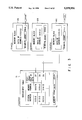
- FIG. 1 is a block diagram showing the construction of a storage system according to an embodiment of the present invention
- FIG. 2 is a block diagram showing a construction of a memory module in connection with the embodiment
- FIG. 3 is a block diagram showing a construction of a memory module in connection with the embodiment
- FIG. 4 is a flowchart for explaining a swapping process associated with the embodiment
- FIGS. 5 and 6 are each flowcharts for explaining a write verify process associated with the embodiment
- FIG. 7 is a diagram for explaining the write voltage control operation in connection with the embodiment.
- FIG. 8 is a flowchart for explaining the write voltage-changing process in connection with the embodiment.
- FIG. 9 is a block diagram for explaining the system of sensing the use rate of the memory module associated with the embodiment.
- FIGS. 10 and 11 are block diagrams for explaining the system of reporting the use rate of the memory module associated with the embodiment
- FIG. 12 is a block diagram for explaining the write inhibit mode associated with the embodiment.
- FIG. 13 is a block diagram showing the construction of an alternative memory block in connection with the embodiment.
- FIG. 14 is a flowchart for explaining a substituting process in connection with the embodiment.
- FIG. 15 is a block diagram showing the construction of a plurality of management tables in connection with the embodiment.
- FIGS. 16A, 16B, 17A, 17B, 18A, and 18B are each perspective views showing the shapes and detachable mechanisms of the memory module associated with the embodiment.
- FIG. 19 is a perspective view showing an outward appearance of a personal computer which is the system body associated with the embodiment.
- This storage system is composed of a memory module 1 made up of flash EEPROMs, a memory controller unit 2, and a host system 3.
- the memory module 1 is a storage system body for storing and retrieving data in response to access by the host system 3 under the control of the controller unit 2.
- the controller unit 2 which is connected to the host system 3 by a data bus 3A, an address bus 3B, and a command bus 3C, transmits and receives data, addresses, and commands.
- the controller unit 2 contains a memory management controller 4, a read/write control circuit 5, an interface controller 6, an ECC (error checking and correcting) circuit 7, a power supply unit 8, and a RAM (random access memory) 9.
- the interface controller 6, which is connected to the host system 3 by the data bus 3A, address bus 3B, and command bus 3C, controls the transfer of data, addresses, and commands to and from the host system 3.
- the read/write control circuit 5, which is connected to the memory module 1 by an address bus 5A, a data bus 5B and a control signal bus 5C, performs read/write control of the memory module 1.
- the control circuit 5 has the function of executing the write verify process and the write voltage-changing process in the write mode.
- the memory management controller 4 executes various memory management processes including the address conversion process, swapping process, memory management information update process, judgment process of memory module 1's using state, and substituting process of memory blocks.
- the RAM 9, which is accessed by the memory management controller 4, is a memory for storing the copies 9A and 9B of a master management table and a management table (see FIG. 2) provided in the memory module 1.
- the address conversion process is a process in which the logical address specified by the host system 3 is converted into a physical address used for accessing the memory module 1.
- the ECC circuit 7, which is connected to the memory management controller 4 and read/write control circuit 5 by a data bus 7A and an address bus 7B, respectively, executes an error checking and correcting process in the data read mode and during the write verify process.
- the power supply unit 8, which has a power supply circuit for supplying a power supply voltage necessary for the read/write operation of the memory module 1, supplies a read voltage Vcc and a write/erase voltage Vpp to the memory module 1.
- the power supply unit 8 is provided with a power supply controller that changes the write/erase voltage Vpp according to the command supplied via the command bus 8A from the read/write control circuit 5.
- the memory module 1 is composed of a plurality of memory blocks of flash EEPROMs arranged in specified units of in-unison erase blocks.
- the memory blocks are divided into a particular memory block used as a master management table 10 that contains master management information, a selected memory block used as a management table 11 that contains memory management information, and a plurality of memory blocks 12A through 12C that store data accessed for writing by the host system 3.
- the master management table 10 is usually a fixed memory block (with physical address 00000), and stores the physical address (12345) of the memory block used for the management table 11.
- the management table 11 stores the management data that is composed of the physical addresses (memory addresses) of the memory blocks 12A through 12C corresponding to the logical addresses (referred to as system addresses) specified by the host system 3, and the high-order data of the rewrite count data for each of the memory block 12A through 12C.
- the management table 11 is not fixed and its physical address is changed by the swapping process explained later.
- the memory blocks 12A through 12C which each have a memory capacity of, for example, 512 bytes of data, store each piece of data on system addresses recognized by the host system 3.
- the memory management controller 4 and read/write control circuit 5 are each composed mainly of a microprocessor.
- the memory management controller 4 of the unit 2 supplies to the read/write control circuit 5 an address for accessing the master management table 10.
- the read/write control circuit 5 reads from the master management table 10 the physical address (12345) of the management table 11 stored, and then transfers it to the memory management controller 4.
- the memory management controller 4 stores the contents of the master management table 10 as copy 9A in the RAM 9A.
- the memory management controller 4 supplies to the read/write control circuit 5 an address for accessing the management table 11 to read in the contents of the management table 11.
- the contents of the management table 11 are stored as copy 9B in the RAM 9.
- the memory management controller 4 secures the management information stored in the memory module 1 beforehand, and executes the memory management of the memory module 1.
- the memory management controller 4 When the host system 3 requests read access to a specified address, the memory management controller 4 refers to the copy 9B in the RAM 9 and converts the specified address (system address) into a physical address in the memory block.
- the read/write control circuit 5 accesses the memory block with the physical address from the memory management controller 4, and reads the stored data from the memory block. For example, as shown in FIG. 2, the read/write control circuit 5 reads the data corresponding to the system address (00312) from the memory block 12A with the physical address (31415).
- the memory management controller 4 transfers the read-out data to the host system 3 via the inter face controller 6 and data bus 3A.
- the memory management controller 4 When the host system 3 requests write access to a specified address, the memory management controller 4 refers to the copy 9B in the RAM 9 and converts the specified address into a physical address in the memory block as described earlier. Based on the physical address, the memory block corresponding to the specified address is accessed. The read/write control circuit 5 erases the contents of the memory block accessed, and then writes the new data transferred from the host system 3 into the memory block.
- the following swap control is executed in order to prevent rewrites from concentrating, in the write mode, on a particular memory block composed of flash EEPROMs whose number of rewrites is limited.
- the management table 11 and memory blocks 12A through 12C in the memory module 1 are each provided with memory areas for storing data on the number of rewrites.
- the rewrite count data is incremented each time a rewrite operation is performed on the memory block accessed.
- the increment process is executed by the memory management controller 4.
- the rewrite count data for each memory block is updated each time the rewrite operation takes place.
- the management table 11 stores the high-order data (of two digits) of the rewrite count data for each of the memory blocks 12A through 12C as well as the rewrite count data of its own.
- the high-order data is not updated each time the write operation occurs, but is updated only when a carry (over two digits in this case) is generated in the rewrite count data.
- the memory management controller 4 accesses the memory block corresponding to the specified address as described in the write mode (steps S1 and S2). Specifically, the memory management controller 4 accesses and reads in, for example, the contents of the memory block 12B via the read/write control circuit 5.
- the memory management controller 4 pays attention to the rewrite count data (3800) in the stored contents, and judges whether or not a carry (a carry over two digits) takes place when the data is incremented (step S4). For the memory block 12B, increment raises the rewrite count data to (3801), causing no carry (NO at step S4). Therefore, as shown in FIG.
- the high-order data (38) corresponding to the memory block 12B in the management table 11 does not change.
- the memory management controller 14 executes a normal write operation, thereby rewriting the data in the memory block 12B accessed to the specified data from the host system 3 (step 5).
- the memory management controller 4 updates the rewrite count data for the memory block 12B to (3801).
- the memory management controller 4 executes the swapping process of swapping memory blocks on the basis of the high-order data in the rewrite count data in the management table.
- the memory management controller 4 executes the swapping of the memory block 12A and memory block 12C (step S7).
- the memory management controller 4 rewrites the contents of the management table 11 as shown in FIG. 3 (step S8).
- the rewrite count data in the management table 11 is also incremented to update the rewrite count data in FIG. 2 from (2528) to (2529).
- Such a swapping process prevents rewrites from concentrating on a particular memory block (for example, 12A), with the result that the rewrite frequency (the high-order data of the rewrite count) of each memory block is equalized.
- the rewrite frequency the high-order data of the rewrite count
- the service life of the respective memory blocks can be lengthened.
- the swapping operation will not be executed, and the data is written, without any modification, into the memory block accessed. It is desirable that the high-order data (38) for the memory block 12C to be swapped should be incremented in the swapping process. This is because a memory block to be swapped will be selected repeatedly in the next swapping process if the value of the high-order data is small.
- each of the memory blocks 12A through 12C stores all the digits of the rewrite count data
- the data of the lower two digits may be stored instead. This introduces no problem in the swapping process, because the management table 11 stores the data of the upper two digits. With this configuration, the memory area for the rewrite count data for each of the memory blocks 12A to 12C can be reduced, so that it is possible to store the more of the other data.
- the read/write control circuit 5 uses a previously prepared program, executes the write verify process of checking to see if writing is done properly, during the write operation in the write mode (see FIGS. 5 and 6).
- the read/write control circuit 5 writes specified data D1 into the memory block corresponding to the specified address (step S10). At this time, the read/write control circuit 5 reads data D2 (write data D1) from the memory block accessed (step S11). The read/write control circuit 5 compares the read-out data D2 with the original data D1 (step S12). If the result of comparison is agreement (YES at step S13), this means that the write operation is performed properly and the writing is terminated.
- the read/write control circuit 5 senses the number of error bits in the read-out data D2 obtained from the comparison, the error distribution, and others. Based on the number of error bits, error distribution, and others, the ECC circuit 7 judges whether or not the error correction process can restore the read-out data D2 to the proper data (step S14). Specifically, it is judged whether or not the error state of the data D2 meets the ECC conditions of the ECC circuit 7. If the conditions are met (YES at step S15), the read/write control circuit 5 will determine that the write operation is done properly and terminate the operation.
- the ECC circuit 7 may perform the ECC process directly on the data D2.
- the read/write control circuit 5 writes the data D1 from the host system 3, and reads the data D2 (write data D1) from the memory block accessed (steps S20 and S21), as shown in FIG. 6.
- This read-out data D2 is supplied to the ECC circuit 7.
- the ECC circuit 7 executes the ECC process, and then supplies the data D2 to the read/write control circuit 5 (step S22).
- the read/write control circuit 5 compares the data D2 subjected to the ECC process with the original data D1 (step S23). If the result of comparison is agreement (YES at step S24), this means that the write operation is done properly, and the writing is terminated.
- the read/write control circuit 5 will repeat the write operation on the data D1. At this time, the read/write control circuit 5 controls the power supply unit 8 so as to raise the write voltage gradually in a range free from excessive writing in the course of repeating the write verify process (see step S34 in FIG. 8).
- the writing may be continued at the present write voltage for the cells judged to be about to finish being written into, whereas a higher voltage may be applied to write data into the cells judged to take some time to finish being written into.
- a higher voltage may be applied to write data into the cells judged to take some time to finish being written into.
- the reading margin may be obtained by the shift control of the threshold voltage or by the shift control combined with ECC, with the read voltage Vcc remaining at 3 V, or a step-up unit may be provided internally to convert the read voltage Vcc into the optimum value for data reading.
- writing data it is possible to set the writing level based on this function. It is also possible to perform the ECC operation using the information obtained from the function. Specifically, after data that becomes unstable due to voltage drift is judged to have a chance to be erroneous, and stable data is judged to be correct data, the ECC operation is continued.
- the ECC circuit 7 performs an ECC operation on the write data and delivers the resulting data to the read/write control circuit 5.
- the ECC circuit 7 also performs an ECC operation on the read-out data to restore it to the original data.
- the method of including compensation data for an error place that appears as an unstable bit in the write operation may be considered instead of ECC that corrects an error in an unspecified place. Since ECC provides error signs of unidirectional error representation (such as a case where the erasing is complete but the writing is incomplete), this assures efficient operations differently from ordinary ECC.
- the memory management controller 4 is provided with a memory 4A that senses the use rate of each memory block (in other words, the consumption rate) and stores each consumption rate sensed, as shown in FIG. 9.
- the memory management controller 4 notifies the host system 3 of the sensed use rate via the interface controller 6.
- the memory management controller 4 senses the use rate of each memory block on the basis of the high-order data of the rewrite count data for each memory block stored in the management table 11, the number of writes repeated until the write verify process is completed, and the number of error bits at the time when the write verify process has finished.
- the number of writes repeated is counted by a counter (A) 50 provided for the read/write control circuit 5.
- the number of error bits is counted by a counter (B) 51 provided for the read/write control circuit 5.
- the memory management controller 4 stores in the memory 4A a table 4B whose data storage addresses are composed of tracks and sectors.
- the table 4B is accessed by the host system 3.
- the memory management controller 4 stores the sensed use rate data 40 at a particular address in table 4B (here, sector 5 on track 11). By accessing the particular address, the host system 3 reads in the use rate data 40 and recognizes the use rate of the corresponding memory block.
- a system may be considered which transfers the use rate data 40 to the host system 3 by the command "Identify Drive” using, for example, an IDE interface.
- the memory 4A is provided with a sector buffer 4c, in which the use rate data 40 is stored as a piece of parameter information.
- the host system 3 accesses the register group in the HDD through program I/O. Each register is selected by address signals and chip select signals.
- a command register one of the register group, is a register into which a command that actuates the HDD is written.
- the drive supports 13 types of commands, one of which is "Identify Drive.” This command is for transferring the parameter information on the HDD to the host system. Once "Identify Drive" has been executed, the parameter information in the HDD is entered in the sector buffer.
- FIG. 10 As for a system that repeats the use rate of the memory block not to the host system but directly to the user, there is a system using a printer 60 as shown in FIG. 10.
- the memory management controller 4 supplies to the printer 60 the print signal corresponding to the sensed use rate of the memory block.
- the printer 60 is positioned so as to come into contact with the printing portion on the surface of the memory module 1. Heat-sensitive paper is placed on the printing portion 1A.
- the printer 60 prints the use rate data on heat-sensitive paper on the printing portion 1A according to the print signal from the memory management controller 4. This enables the user to know from the result the use rate of the memory block.
- the memory management controller 4 stores message data in, for example, the management table 11 in the memory block 1.
- This message data is the voice information that informs the user of the use rate of the memory block sensed by the memory management controller 4.
- the memory controller 2 which contains a D/A (digital-to-analog) converter 71, D/A converts the voice information read from the memory module 1 and sends the resulting signal to the voice output unit 70.
- the voice output unit 70 which is made up of an amplifier and a speaker, supplies the use rate of the memory block in voice.
- the voice information is allowed to include information that first sounds a buzzer or the like. Further, because the user cannot understand what has been said if the system spoke without notice, the voice information is allowed to contain information that identifies itself as a semiconductor disk device being a sound source. In case of a failure, information on the telephone number of the service center and others is included in the voice information.
- a voice is produced in such a manner that when the use still continues even after an alarm has been given in voice, another alarm is raised in every write operation (especially when the writing intervals are short, an alarm is given in regular intervals of several seconds), that the contents of a voice are varied with the remaining life, or that the interval between alarms is changed.
- the memory management controller 4 which contains a comparator 4D, has the function of comparing the write data at the specified address with the recorded data already existing at the same address at the time of write access by the host system 3.
- the memory management controller 4 reads out the data D2 already stored in the memory block 12A.
- the comparator 4D of the memory management controller 4 compares the read-out data D2 with the write data D1 from the host system 3. If the result of the comparison is disagreement, the memory management controller 4 executes the write mode to perform the operation of writing the write data D1 into the memory block 12A.
- the memory management controller 4 judges that the address being accessed has already stored the data D2 identical with the specified data D1, and inhibits an actual write operation. Specifically, the memory management controller 4 terminates the write operation without supplying the physical address corresponding to the logical address being accessed to the read/write control circuit 5 (reporting the completion of writing to the host system 3). Therefore, when the data identical with the data being write-accessed has already written, the write operation can be omitted, with the result that the number of rewrites for the memory block can be reduced.
- Such a function of inhibiting the writing of the same write data is called a self-compare write function.
- the self-compare write function is selected as desired by commands or the like from the host system 3.
- the memory module 1 is provided with a plurality of alternative memory blocks 80A through 80C. Using those alternative memory blocks 80A through 80C, the memory management controller 4 executes a substituting process as shown in FIG. 14.
- the memory management controller 4 accesses the memory block corresponding to the specified address (steps S40 and S41).
- the memory management controller 4 erases the stored data in, for example, the memory block 12A accessed, via the read/write control circuit 5 (step S42).
- the memory management controller 4 will execute the process of switching the memory block 12A to, for example, an alternative memory block 80A (YES at step S43, and step S45).
- the contents of the management table 11 are rewritten so that the physical address of the memory block 12A corresponding to the system address (logical address) from the host system 3 may be converted into the physical address of the alternative memory block 80A. This eliminates the system address corresponding to the physical address of the memory block 12A in which an error occurred.
- the read/write control circuit 5 writes the write data from the host system 3 into the alternative memory block 80A (step S46). On the other hand, when no error has occurred, the read/write control circuit 5 writes specified write data into the memory block 12A accessed (NO at step S43, and step S44).
- the write data from the host system 3 can be protected when a writing error has occurred in the memory block accessed in the write mode, by writing the data in the alternative memory block.
- One of the causes of writing errors may be a case where a memory block whose number of rewrites has exceeded its limit is accessed.
- the alternative memory block 80C with the lowest substituting priority is allowed to store message information that indicates the life limit of the memory module 1.
- the message information is read from the memory block 80C to notify the user of the fact. The notification is made in a voice as shown in FIG. 11. After the message information has been reported to the user, the alternative memory block 80C is used as a normal alternative memory block.
- the memory module 1 may have a plurality of management tables 11A through 11C.
- Each of management tables 11A through 11C stores management information that manages a plurality of corresponding memory blocks.
- the master management table 10 stores the physical address of each of management tables 11A through 11C.
- each of the management tables 11A through 11C stores the management information allocated with the system address in the host system 3 on the basis of the physical address of each of the memory blocks. That is, the physical address is fixed and the system address is made variable. With this system, a swapping process can be carried out so as to equalize the access frequency for the physical address of each memory block.
- the memory management controller 4 copies the contents of each of management tables 11A through 11C into the RAM 9. At this time, the contents of each of management tables 11A through 11C are sorted, and converted into those based on the system addresses (logical addresses) in the host system 3. This is because the retrieval of physical addresses to be accessed becomes difficult if the operation is based on the physical addresses when the system addresses are supplied from the host system 3.
- a typical thickness of notebook-type personal computers is approximately 44 mm. Some are as thin as 27 mm in thickness. Except for this, most personal computers of this type have a thickness of nearly 44 mm, although similar ones have a thickness of nearly 39 mm at a minimum.
- HDDs are being made more compact and 1.8-inch models are available with a width of nearly 50.8 mm to 54 mm. Therefore, for 1.8-inch HDDs, it is impossible to install the HDD in a notebook-type personal computer so that the width of the HDD may fit in the thickness of the notebook-type personal computer.
- reference character 1 indicates a length and h denotes a height (a thickness).
- a plurality of chips (flash EEPROMs) 90 constituting the memory module 1 are housed in a case 91.
- Each chip 90 is detachably installed in a computer body (system body) 93 by means of a flexible cable 92 attached to the case 91, as shown in FIG. 16B.
- the controller 2 is connected to the memory module 1 to form a disk unit to which the present invention is applied.
- the memory module 1 is placed in series with an additional one with their width aligned with the thickness of the system body 93.
- the memory module 1 may be installed detachably in the system body 93 by means of the flexible cable 92 and a connector 92A.
- the memory module is also arranged in series with an additional one with their width aligned with the thickness of the system body 93.
- the memory module 1 is composed of a memory pack 94 containing a plurality of chips 90.
- the memory pack 94 is provided with contact pins 95 and pin receptacle electrodes 96.
- each memory pack 94 may be installed detachably in the system body 93 via contact pins 95 and pin receptacle electrodes.
- each memory pack 94 is externally added to the system body 93. With such an externally added arrangement, the size of the system body 93 itself can be made smaller than the aforementioned system where the memory module 1 is housed in the system body. Since another memory module 1 can be added as desired and removed easily, it is easy to replace the memory module 1, depending on the consumption state of the memory module 1.
- the system body 93 is, for example, a laptop personal computer as shown in FIG. 19. Installed in the system body 93 is a silicon disk unit 100 containing the memory module 1 and the memory controller 2.
- the consumption state of the flash EEPROMs constituting the memory module is sensed and the state is reported to the host system or the user, this provides for a case where the number of rewrites of the flash EEPROMs has reached its limit as they are used, and writing is finally impossible. This prevents the user from being embarrassed by sudden incapability of writing.
- the memory module 1 has the management table 11 in it, the host system 3 can access the flash EEPROMs in a similar manner to ordinary HDDs without paying attention to the difference between those types of memory elements. Since the memory modules are constructed so as to fit in with the thickness of the system body in a detachable and expandable manner, this achieves the optimum unit dimensions in terms of system installation, being free from the specifications of existing HDDs.
- the controller 2 reads the management information from the memory module 1 at the system start-up, and copies the read-out information in the RAM 9. This allows the memory system to be automatically constructed at the time of the system start-up when memory modules 1 are changed. In other words, when the changing of memory modules 1 is done, the controller 2 realizes a system configuration according to the management information held in the memory module 1 at the time of the start-up of the system power supply.
- the management table 11 prevents accesses from concentrating on a particular memory block in the memory module 1, thereby equalizing the use frequency for each memory block.
- the self-compare write function can inhibit the same data as the existing data from being written at the same address. Therefore, it is possible not only to prevent useless writing to improve the processing speed, but also to lengthen the service life of the memory module.
- the swapping process equalizes the use frequency of each memory block. This prevents the memory module from deteriorating partially, thereby lengthening its service life.
- the write verify process can save the address even if an error has occurred during the data write operation, with the result that the service life of the memory module can be made longer. Since the voltage for data writing is allowed to vary with the writing state of each cell, a cell difficult to write data can be written into at a higher voltage, thereby making use of the writing life to a maximum.
- the consumption state of the memory module is read out and then supplied to the host system, which allows the host system to judge the life of the memory module.
- an alternative memory block is used. This substituting process saves the data even if an unusable memory area (physical address) appears in a part of the memory module, with the result that the service life of the memory module is made longer.
Abstract
In a storage system using flash EEPROMs, a memory module is composed of a plurality of memory blocks arranged in units of in-unison erase blocks. Some of the memory blocks are used as management tables storing management information for managing address allocation of each memory block and the number of rewrites for each memory block. A memory controller reads the management information from the management table at the system start-up, and based on the management information, controls the read/write access to each memory block.
Description
This application is a continuation of application Ser. No. 08/001,750, filed Jan. 7, 1993, now abandoned.
1. Field of the Invention
This invention relates to a storage system with a flash memory module using flash EEPROMs as memory elements, and more particularly to a storage system constituting a silicon disk unit used as an external memory device for a computer system.
2. Description of the Related Art
Flash EEPROMs (electrically erasable and programmable read-only memories) are rewritable nonvolatile memory elements that can be erased over the entire chip or in blocks. There are EEPROMs known to be similar to flash EEPROMs. EEPROMs, which are electrically erasable, differ from flash EEPROMs in that the former are erased in bytes.
Unlike EEPROMs, flash EEPROMs do not require a data erase driving circuit for each memory cell, which allows a construction of a single transistor per memory cell. They, therefore, provide a high packing density like other semiconductor memory devices such as DRAMs and mask ROMs.
Flash EEPROMs are characterized by being rewritable but has the disadvantage that there is a limit to the number of possible rewrites. Specifically, data writing may grow more difficult as it is used further, and eventually impossible. Data writing and erasing are done by applying a high voltage such as 12 V or 20 V to inject charges into or extract charges from the floating gate. In the data write operation, to equalize the cell potentials after writing, a high voltage is generally applied in small time divisions until a specified potential is reached, while the write verify operation is being executed on each memory cell.
Recently, storage systems have been developed which employ flash EEPROMs for an external memory device, called a silicon disk unit, for a computer system. Those storage systems are broadly divided into two types: one type is such that a host system recognizes write information in file form, and writes data into flash EEPROMs in a manner that distinguishes file management information from the contents of files, and the other type is such that a host system does not particularly recognize write information but uses the storage system as an external storage device like a conventional hard disk drive (HDD).
With those types, flash EEPROMs can be used as external storage devices, but there is still a limit to the number of possible rewrites in flash EEPROMs as noted earlier. This creates the problem that when the host system writes data in the external memory system, rewrites can concentrate on a particular block of the flash EEPROMs (an in-unison erase block unit), which makes it impossible to rewrite, thereby leading to a serious reduction in the service life of the entire system. With the first type, it is possible to alleviate the concentration of rewrites on a particular block by causing the host system to select a file storage location. To do this, however, the host system needs software to manage the number of rewrites, thereby falling short of universality.
Additionally, when the host system accesses the external storage system, address allocation management is necessary which converts logical addresses in the host system into physical addresses in blocks of flash EEPROMs. Conventionally, because the host system must perform the address allocation management, the system without address allocation management software cannot handle such a memory system, thus leading to lack of universality as mentioned above.
An object of the present invention is to prevent a situation where rewrites concentrate on a particular block of flash EEPROMs, without management by the host system, in a storage system that uses flash EEPROMs as an external memory system for a computer system.
Another object of the present invention is to provide a storage system that can be accessed by logical addresses in the host system like an ordinary external storage system, without address allocation by the host system.
The foregoing objects are accomplished by providing a storage system comprising: a memory module composed of a plurality of memory blocks arranged in units of in-unison erase blocks; memory management means composed of memory management memory blocks, selected from each of the memory blocks, which store management information that manages address allocation of each of the memory blocks; and memory controller means which executes memory control in a manner that, based on the management information stored in the memory management memory block, reads the data at the address specified by the host system from a memory block of the flash memory module, or writes specified data in the memory block corresponding to the specified address. It further comprises rewrite count data memory means which stores the rewrite count data for each memory block updated when data is rewritten. The memory management means stores management information that manages the rewrite frequency for each memory block on the basis of the rewrite count data.
Additional objects and advantages of the invention will be set forth in the description which follows, and in part will be obvious from the description, or may be learned by practice of the invention. The objects and advantages of the invention may be realized and obtained by means of the instrumentalities and combinations particularly pointed out in the appended claims.
The accompanying drawings, which are incorporated in and constitute a part of the specification, illustrate presently preferred embodiments of the invention, and together with the general description given above and the detailed description of the preferred embodiments given below, serve to explain the principles of the invention.
FIG. 1 is a block diagram showing the construction of a storage system according to an embodiment of the present invention;
FIG. 2 is a block diagram showing a construction of a memory module in connection with the embodiment;
FIG. 3 is a block diagram showing a construction of a memory module in connection with the embodiment;
FIG. 4 is a flowchart for explaining a swapping process associated with the embodiment;
FIGS. 5 and 6 are each flowcharts for explaining a write verify process associated with the embodiment;
FIG. 7 is a diagram for explaining the write voltage control operation in connection with the embodiment;
FIG. 8 is a flowchart for explaining the write voltage-changing process in connection with the embodiment;
FIG. 9 is a block diagram for explaining the system of sensing the use rate of the memory module associated with the embodiment;
FIGS. 10 and 11 are block diagrams for explaining the system of reporting the use rate of the memory module associated with the embodiment;
FIG. 12 is a block diagram for explaining the write inhibit mode associated with the embodiment;
FIG. 13 is a block diagram showing the construction of an alternative memory block in connection with the embodiment;
FIG. 14 is a flowchart for explaining a substituting process in connection with the embodiment;
FIG. 15 is a block diagram showing the construction of a plurality of management tables in connection with the embodiment;
FIGS. 16A, 16B, 17A, 17B, 18A, and 18B are each perspective views showing the shapes and detachable mechanisms of the memory module associated with the embodiment; and
FIG. 19 is a perspective view showing an outward appearance of a personal computer which is the system body associated with the embodiment.
Referring to the accompanying drawings, a storage system according an embodiment of the present invention will be explained hereinafter.
Basic Configuration of the System
This storage system, as shown in FIG. 1, is composed of a memory module 1 made up of flash EEPROMs, a memory controller unit 2, and a host system 3. The memory module 1 is a storage system body for storing and retrieving data in response to access by the host system 3 under the control of the controller unit 2.
The controller unit 2, which is connected to the host system 3 by a data bus 3A, an address bus 3B, and a command bus 3C, transmits and receives data, addresses, and commands.
The controller unit 2 contains a memory management controller 4, a read/write control circuit 5, an interface controller 6, an ECC (error checking and correcting) circuit 7, a power supply unit 8, and a RAM (random access memory) 9.
The interface controller 6, which is connected to the host system 3 by the data bus 3A, address bus 3B, and command bus 3C, controls the transfer of data, addresses, and commands to and from the host system 3. The read/write control circuit 5, which is connected to the memory module 1 by an address bus 5A, a data bus 5B and a control signal bus 5C, performs read/write control of the memory module 1. The control circuit 5 has the function of executing the write verify process and the write voltage-changing process in the write mode.
The memory management controller 4, according to the memory management information stored in the RAM 9, executes various memory management processes including the address conversion process, swapping process, memory management information update process, judgment process of memory module 1's using state, and substituting process of memory blocks. The RAM 9, which is accessed by the memory management controller 4, is a memory for storing the copies 9A and 9B of a master management table and a management table (see FIG. 2) provided in the memory module 1. The address conversion process is a process in which the logical address specified by the host system 3 is converted into a physical address used for accessing the memory module 1.
The ECC circuit 7, which is connected to the memory management controller 4 and read/write control circuit 5 by a data bus 7A and an address bus 7B, respectively, executes an error checking and correcting process in the data read mode and during the write verify process. The power supply unit 8, which has a power supply circuit for supplying a power supply voltage necessary for the read/write operation of the memory module 1, supplies a read voltage Vcc and a write/erase voltage Vpp to the memory module 1. The power supply unit 8 is provided with a power supply controller that changes the write/erase voltage Vpp according to the command supplied via the command bus 8A from the read/write control circuit 5.
The memory module 1 is composed of a plurality of memory blocks of flash EEPROMs arranged in specified units of in-unison erase blocks. In this invention, the memory blocks are divided into a particular memory block used as a master management table 10 that contains master management information, a selected memory block used as a management table 11 that contains memory management information, and a plurality of memory blocks 12A through 12C that store data accessed for writing by the host system 3.
The master management table 10 is usually a fixed memory block (with physical address 00000), and stores the physical address (12345) of the memory block used for the management table 11. The management table 11 stores the management data that is composed of the physical addresses (memory addresses) of the memory blocks 12A through 12C corresponding to the logical addresses (referred to as system addresses) specified by the host system 3, and the high-order data of the rewrite count data for each of the memory block 12A through 12C. The management table 11 is not fixed and its physical address is changed by the swapping process explained later. The memory blocks 12A through 12C, which each have a memory capacity of, for example, 512 bytes of data, store each piece of data on system addresses recognized by the host system 3.
The memory management controller 4 and read/write control circuit 5 are each composed mainly of a microprocessor.
A basic operation of a system thus constructed will be explained.
System Start-Up Mode
At the time of system start-up, the memory management controller 4 of the unit 2 supplies to the read/write control circuit 5 an address for accessing the master management table 10. The read/write control circuit 5 reads from the master management table 10 the physical address (12345) of the management table 11 stored, and then transfers it to the memory management controller 4. The memory management controller 4 stores the contents of the master management table 10 as copy 9A in the RAM 9A.
Further, the memory management controller 4 supplies to the read/write control circuit 5 an address for accessing the management table 11 to read in the contents of the management table 11. The contents of the management table 11 are stored as copy 9B in the RAM 9. In the start-up mode, the memory management controller 4 secures the management information stored in the memory module 1 beforehand, and executes the memory management of the memory module 1.
Read Mode
When the host system 3 requests read access to a specified address, the memory management controller 4 refers to the copy 9B in the RAM 9 and converts the specified address (system address) into a physical address in the memory block. The read/write control circuit 5 accesses the memory block with the physical address from the memory management controller 4, and reads the stored data from the memory block. For example, as shown in FIG. 2, the read/write control circuit 5 reads the data corresponding to the system address (00312) from the memory block 12A with the physical address (31415). The memory management controller 4 transfers the read-out data to the host system 3 via the inter face controller 6 and data bus 3A.
Write Mode
When the host system 3 requests write access to a specified address, the memory management controller 4 refers to the copy 9B in the RAM 9 and converts the specified address into a physical address in the memory block as described earlier. Based on the physical address, the memory block corresponding to the specified address is accessed. The read/write control circuit 5 erases the contents of the memory block accessed, and then writes the new data transferred from the host system 3 into the memory block.
Swap Control Mode
In the present invention, the following swap control is executed in order to prevent rewrites from concentrating, in the write mode, on a particular memory block composed of flash EEPROMs whose number of rewrites is limited.
As shown in FIG. 3, the management table 11 and memory blocks 12A through 12C in the memory module 1 are each provided with memory areas for storing data on the number of rewrites. The rewrite count data is incremented each time a rewrite operation is performed on the memory block accessed. The increment process is executed by the memory management controller 4. The rewrite count data for each memory block is updated each time the rewrite operation takes place.
The management table 11 stores the high-order data (of two digits) of the rewrite count data for each of the memory blocks 12A through 12C as well as the rewrite count data of its own. The high-order data is not updated each time the write operation occurs, but is updated only when a carry (over two digits in this case) is generated in the rewrite count data.
On the assumption described above, when the host system 3 requests write access to a specified address as shown in FIG. 4, the memory management controller 4 accesses the memory block corresponding to the specified address as described in the write mode (steps S1 and S2). Specifically, the memory management controller 4 accesses and reads in, for example, the contents of the memory block 12B via the read/write control circuit 5. The memory management controller 4 pays attention to the rewrite count data (3800) in the stored contents, and judges whether or not a carry (a carry over two digits) takes place when the data is incremented (step S4). For the memory block 12B, increment raises the rewrite count data to (3801), causing no carry (NO at step S4). Therefore, as shown in FIG. 3, the high-order data (38) corresponding to the memory block 12B in the management table 11 does not change. In this way, when no carry takes place, the memory management controller 14 executes a normal write operation, thereby rewriting the data in the memory block 12B accessed to the specified data from the host system 3 (step 5). At this time, the memory management controller 4 updates the rewrite count data for the memory block 12B to (3801).
when the memory block corresponding to the specified address is the memory block 12A as shown in FIG. 3, increment raises the rewrite count data from (3899) to (3900), generating a carry (YES at step S4). In this case, the memory management controller 4 executes the swapping process of swapping memory blocks on the basis of the high-order data in the rewrite count data in the management table.
Specifically, the difference between the high-order data in the memory block 12A and the smallest of the high-order data in the other memory blocks is 2 or more, the memory block with the smallest high-order data is selected (step S6). Here, the memory block 12C with the physical address (58979) has the smallest high-order data (37). Thus, the memory management controller 4 executes the swapping of the memory block 12A and memory block 12C (step S7). By this swapping process, the memory management controller 4 rewrites the contents of the management table 11 as shown in FIG. 3 (step S8). At this time, the rewrite count data in the management table 11 is also incremented to update the rewrite count data in FIG. 2 from (2528) to (2529).
By the swapping process, data to be written into the system address (00312) is written into the memory block 12C. Before the writing, the data at the system address (02312) that is the contents of the memory block 12C is written into the memory block 12A. Therefore, the rewrite count data for each of the memory blocks 12A and 12C is incremented. With the updated management table 11 (see FIG. 3), when the system address (00312) is specified in the next write access, the memory block 12C is accessed. When the system address (02312) is specified, the memory block 12A is accessed.
Such a swapping process prevents rewrites from concentrating on a particular memory block (for example, 12A), with the result that the rewrite frequency (the high-order data of the rewrite count) of each memory block is equalized. As mentioned earlier, since there is a limit to the number of rewrites in flash EEPROMs constituting the memory blocks, if rewrites concentrate on a particular memory block, it will be impossible to rewrite the contents of the memory block. Thus, by equalizing the rewrite frequency of each memory block, the service life of the respective memory blocks can be lengthened.
Here, when the difference from the value of the smallest high-order data is less than 2, the swapping operation will not be executed, and the data is written, without any modification, into the memory block accessed. It is desirable that the high-order data (38) for the memory block 12C to be swapped should be incremented in the swapping process. This is because a memory block to be swapped will be selected repeatedly in the next swapping process if the value of the high-order data is small.
Although each of the memory blocks 12A through 12C stores all the digits of the rewrite count data, the data of the lower two digits may be stored instead. This introduces no problem in the swapping process, because the management table 11 stores the data of the upper two digits. With this configuration, the memory area for the rewrite count data for each of the memory blocks 12A to 12C can be reduced, so that it is possible to store the more of the other data.
Write Verify Process
In the present invention, the read/write control circuit 5, using a previously prepared program, executes the write verify process of checking to see if writing is done properly, during the write operation in the write mode (see FIGS. 5 and 6).
As shown in FIG. 5, to meet the write access request from the host system 3, the read/write control circuit 5 writes specified data D1 into the memory block corresponding to the specified address (step S10). At this time, the read/write control circuit 5 reads data D2 (write data D1) from the memory block accessed (step S11). The read/write control circuit 5 compares the read-out data D2 with the original data D1 (step S12). If the result of comparison is agreement (YES at step S13), this means that the write operation is performed properly and the writing is terminated.
On the other hand, if the comparison result is disagreement (NO at step S13), the read/write control circuit 5 senses the number of error bits in the read-out data D2 obtained from the comparison, the error distribution, and others. Based on the number of error bits, error distribution, and others, the ECC circuit 7 judges whether or not the error correction process can restore the read-out data D2 to the proper data (step S14). Specifically, it is judged whether or not the error state of the data D2 meets the ECC conditions of the ECC circuit 7. If the conditions are met (YES at step S15), the read/write control circuit 5 will determine that the write operation is done properly and terminate the operation. With this process, the number of write operations by the write verify process (the number of rewrites) can be reduced as long as the occurrence of errors is within a permitted limit, which prevents the write verify process from shortening the service life of the memory blocks. Here, in the judgment based on the ECC conditions, the ECC circuit 7 may perform the ECC process directly on the data D2.
In another approach, the read/write control circuit 5 writes the data D1 from the host system 3, and reads the data D2 (write data D1) from the memory block accessed (steps S20 and S21), as shown in FIG. 6. This read-out data D2 is supplied to the ECC circuit 7. The ECC circuit 7 executes the ECC process, and then supplies the data D2 to the read/write control circuit 5 (step S22). The read/write control circuit 5 compares the data D2 subjected to the ECC process with the original data D1 (step S23). If the result of comparison is agreement (YES at step S24), this means that the write operation is done properly, and the writing is terminated.
On the other hand, if the comparison result is disagreement (NO at step S24), the read/write control circuit 5 will repeat the write operation on the data D1. At this time, the read/write control circuit 5 controls the power supply unit 8 so as to raise the write voltage gradually in a range free from excessive writing in the course of repeating the write verify process (see step S34 in FIG. 8).
Because of the properties of flash EEPROMs, the charge movement during the data writing varies with the applied voltage. Therefore, if the write voltage is variable, data can be written at higher voltages into cells difficult to write in, allowing for maximum use of the writing life. It can also be expected that the sum of repeated write times is shortened. As to voltage-raising steps, there is no problem as long as the voltage is raised stepwise, with each step being smaller than variations in the step-up unit for generating the write voltage Vpp built in the existing chips.
For another system, by shifting the threshold voltage for the data read operation as shown in FIG. 7, according to the writing state of the cell, at the time of reading for the write verify process, the writing may be continued at the present write voltage for the cells judged to be about to finish being written into, whereas a higher voltage may be applied to write data into the cells judged to take some time to finish being written into. Namely, in FIG. 7, when a cell is in the writing state indicated by A, writing may be done at a normal voltage, and when a cell is in a state indicated by B, writing may be done at a higher voltage.
In threshold voltage setting during a normal data read operation, when data cannot be read out as expected (such as when an incurable error has been found in the ECC process), the threshold voltage is drifted for reading. This assures margins and 3-V logic levels. To realize a semiconductor disk device with 3-V external power supply specification, the reading margin may be obtained by the shift control of the threshold voltage or by the shift control combined with ECC, with the read voltage Vcc remaining at 3 V, or a step-up unit may be provided internally to convert the read voltage Vcc into the optimum value for data reading.
In writing data, it is possible to set the writing level based on this function. It is also possible to perform the ECC operation using the information obtained from the function. Specifically, after data that becomes unstable due to voltage drift is judged to have a chance to be erroneous, and stable data is judged to be correct data, the ECC operation is continued.
Here, the ECC circuit 7 performs an ECC operation on the write data and delivers the resulting data to the read/write control circuit 5. The ECC circuit 7 also performs an ECC operation on the read-out data to restore it to the original data. On the assumption that no error will occur in the read operation when the flash EEPROM operates properly in the write verify operation, the method of including compensation data for an error place that appears as an unstable bit in the write operation may be considered instead of ECC that corrects an error in an unspecified place. Since ECC provides error signs of unidirectional error representation (such as a case where the erasing is complete but the writing is incomplete), this assures efficient operations differently from ordinary ECC.
Sensing the Use Rate of Memory Blocks
The memory management controller 4 is provided with a memory 4A that senses the use rate of each memory block (in other words, the consumption rate) and stores each consumption rate sensed, as shown in FIG. 9. The memory management controller 4 notifies the host system 3 of the sensed use rate via the interface controller 6.
The memory management controller 4 senses the use rate of each memory block on the basis of the high-order data of the rewrite count data for each memory block stored in the management table 11, the number of writes repeated until the write verify process is completed, and the number of error bits at the time when the write verify process has finished. The number of writes repeated is counted by a counter (A) 50 provided for the read/write control circuit 5. The number of error bits is counted by a counter (B) 51 provided for the read/write control circuit 5.
As shown in FIG. 9, when the memory module 1 is used as a disk unit similar to an HDD, the memory management controller 4 stores in the memory 4A a table 4B whose data storage addresses are composed of tracks and sectors. The table 4B is accessed by the host system 3. The memory management controller 4 stores the sensed use rate data 40 at a particular address in table 4B (here, sector 5 on track 11). By accessing the particular address, the host system 3 reads in the use rate data 40 and recognizes the use rate of the corresponding memory block.
As an interface with the host system 3, a system may be considered which transfers the use rate data 40 to the host system 3 by the command "Identify Drive" using, for example, an IDE interface. In this system, as shown FIG. 9, the memory 4A is provided with a sector buffer 4c, in which the use rate data 40 is stored as a piece of parameter information.
In the IDE interface system, the host system 3 accesses the register group in the HDD through program I/O. Each register is selected by address signals and chip select signals. A command register, one of the register group, is a register into which a command that actuates the HDD is written. The drive supports 13 types of commands, one of which is "Identify Drive." This command is for transferring the parameter information on the HDD to the host system. Once "Identify Drive" has been executed, the parameter information in the HDD is entered in the sector buffer.
As for a system that repeats the use rate of the memory block not to the host system but directly to the user, there is a system using a printer 60 as shown in FIG. 10. In this system, the memory management controller 4 supplies to the printer 60 the print signal corresponding to the sensed use rate of the memory block. The printer 60 is positioned so as to come into contact with the printing portion on the surface of the memory module 1. Heat-sensitive paper is placed on the printing portion 1A. The printer 60 prints the use rate data on heat-sensitive paper on the printing portion 1A according to the print signal from the memory management controller 4. This enables the user to know from the result the use rate of the memory block.
For a system that reports directly to the user, there is a voice output unit 70 as shown in FIG. 11. In this system, the memory management controller 4 stores message data in, for example, the management table 11 in the memory block 1. This message data is the voice information that informs the user of the use rate of the memory block sensed by the memory management controller 4.
The memory controller 2, which contains a D/A (digital-to-analog) converter 71, D/A converts the voice information read from the memory module 1 and sends the resulting signal to the voice output unit 70. The voice output unit 70, which is made up of an amplifier and a speaker, supplies the use rate of the memory block in voice.
Since, for example, the user may be surprised if the system starts to speak suddenly, the voice information is allowed to include information that first sounds a buzzer or the like. Further, because the user cannot understand what has been said if the system spoke without notice, the voice information is allowed to contain information that identifies itself as a semiconductor disk device being a sound source. In case of a failure, information on the telephone number of the service center and others is included in the voice information. A voice is produced in such a manner that when the use still continues even after an alarm has been given in voice, another alarm is raised in every write operation (especially when the writing intervals are short, an alarm is given in regular intervals of several seconds), that the contents of a voice are varied with the remaining life, or that the interval between alarms is changed.
Write Inhibit Mode
As shown in FIG. 12, the memory management controller 4, which contains a comparator 4D, has the function of comparing the write data at the specified address with the recorded data already existing at the same address at the time of write access by the host system 3. When, for example, the memory block 12A in the memory module 1 is write-accessed by the specified address from the host system 1, the memory management controller 4 reads out the data D2 already stored in the memory block 12A. The comparator 4D of the memory management controller 4 compares the read-out data D2 with the write data D1 from the host system 3. If the result of the comparison is disagreement, the memory management controller 4 executes the write mode to perform the operation of writing the write data D1 into the memory block 12A.
On the other hand, if the comparison result is agreement, the memory management controller 4 judges that the address being accessed has already stored the data D2 identical with the specified data D1, and inhibits an actual write operation. Specifically, the memory management controller 4 terminates the write operation without supplying the physical address corresponding to the logical address being accessed to the read/write control circuit 5 (reporting the completion of writing to the host system 3). Therefore, when the data identical with the data being write-accessed has already written, the write operation can be omitted, with the result that the number of rewrites for the memory block can be reduced. Such a function of inhibiting the writing of the same write data is called a self-compare write function. The self-compare write function is selected as desired by commands or the like from the host system 3.
Alternative Memory Block
As shown in FIG. 13, the memory module 1 is provided with a plurality of alternative memory blocks 80A through 80C. Using those alternative memory blocks 80A through 80C, the memory management controller 4 executes a substituting process as shown in FIG. 14.
As shown in FIG. 14, when the host system 3 requests write access to a specified address, the memory management controller 4 accesses the memory block corresponding to the specified address (steps S40 and S41). The memory management controller 4 erases the stored data in, for example, the memory block 12A accessed, via the read/write control circuit 5 (step S42). In erasing the data or during the write verify operation, if an error takes place in the memory block 12A, the memory management controller 4 will execute the process of switching the memory block 12A to, for example, an alternative memory block 80A (YES at step S43, and step S45). Specifically, the contents of the management table 11 are rewritten so that the physical address of the memory block 12A corresponding to the system address (logical address) from the host system 3 may be converted into the physical address of the alternative memory block 80A. This eliminates the system address corresponding to the physical address of the memory block 12A in which an error occurred.
Based on the management table 11, the read/write control circuit 5 writes the write data from the host system 3 into the alternative memory block 80A (step S46). On the other hand, when no error has occurred, the read/write control circuit 5 writes specified write data into the memory block 12A accessed (NO at step S43, and step S44).
With such a substituting process using the alternative memory blocks 80A through 80C, the write data from the host system 3 can be protected when a writing error has occurred in the memory block accessed in the write mode, by writing the data in the alternative memory block. One of the causes of writing errors may be a case where a memory block whose number of rewrites has exceeded its limit is accessed.
There is a system which has a substituting sequence of the alternative memory blocks 80A through 80C. Of those alternative memory blocks 80A through 80C, the alternative memory block 80C with the lowest substituting priority is allowed to store message information that indicates the life limit of the memory module 1. When the number of remaining memory blocks decreases as a result of substituting processes, that is, when the memory module 1 comes closer to its life limit, the message information is read from the memory block 80C to notify the user of the fact. The notification is made in a voice as shown in FIG. 11. After the message information has been reported to the user, the alternative memory block 80C is used as a normal alternative memory block.
A Plurality of Management Tables
As shown in FIG. 15, the memory module 1 may have a plurality of management tables 11A through 11C. Each of management tables 11A through 11C stores management information that manages a plurality of corresponding memory blocks. The master management table 10 stores the physical address of each of management tables 11A through 11C.
In such a system, when physical addresses are allocated to the respective memory blocks on the basis of the system addresses in the host system 3, a management table with a system address frequently accessed undergoes a swapping operation more often. This raises the problem that the number of rewrites (rewrite frequency) differs greatly from one memory block to another in each of the management tables 11A through 11C. To solve such a problem, each of the management tables 11A through 11C stores the management information allocated with the system address in the host system 3 on the basis of the physical address of each of the memory blocks. That is, the physical address is fixed and the system address is made variable. With this system, a swapping process can be carried out so as to equalize the access frequency for the physical address of each memory block.
In the system start-up, the memory management controller 4 copies the contents of each of management tables 11A through 11C into the RAM 9. At this time, the contents of each of management tables 11A through 11C are sorted, and converted into those based on the system addresses (logical addresses) in the host system 3. This is because the retrieval of physical addresses to be accessed becomes difficult if the operation is based on the physical addresses when the system addresses are supplied from the host system 3.
The Shape and Detachable Mechanism of Memory Module 1
Presently, a typical thickness of notebook-type personal computers is approximately 44 mm. Some are as thin as 27 mm in thickness. Except for this, most personal computers of this type have a thickness of nearly 44 mm, although similar ones have a thickness of nearly 39 mm at a minimum. HDDs are being made more compact and 1.8-inch models are available with a width of nearly 50.8 mm to 54 mm. Therefore, for 1.8-inch HDDs, it is impossible to install the HDD in a notebook-type personal computer so that the width of the HDD may fit in the thickness of the notebook-type personal computer.
In the case of a silicon disk unit to which the present invention has been applied, however, it is possible to install an HDD with its width aligned with the thickness of a notebook-type personal computer. In this case, to assure marketability, it is necessary to take into account the thinnest of similar models at present, whose thickness is as thin as 39 mm.
In this case, when a disk unit of the present invention is installed, the personal computer requires 1.5 mm for the outer casing and 0.5 mm for clearance, that is, a total of 2 mm on each side. Therefore, as shown in FIGS. 16A and 16B, to fit the unit in a thickness of 39 mm, the width w of the disk unit (the width of the memory module 1) must be designed to be smaller than 39-2-2=35 mm. Installing the unit this way provides the advantage of securing an area for the main board on the personal computer side. In the figure, reference character 1 indicates a length and h denotes a height (a thickness).
As shown in FIG. 16A, a plurality of chips (flash EEPROMs) 90 constituting the memory module 1 are housed in a case 91. Each chip 90 is detachably installed in a computer body (system body) 93 by means of a flexible cable 92 attached to the case 91, as shown in FIG. 16B. Inside the computer body 93, the controller 2 is connected to the memory module 1 to form a disk unit to which the present invention is applied. In this case, the memory module 1 is placed in series with an additional one with their width aligned with the thickness of the system body 93.
As shown in FIGS. 17A and 17B, the memory module 1 may be installed detachably in the system body 93 by means of the flexible cable 92 and a connector 92A. In this case, the memory module is also arranged in series with an additional one with their width aligned with the thickness of the system body 93.
As shown in FIG. 18A, the memory module 1 is composed of a memory pack 94 containing a plurality of chips 90. The memory pack 94 is provided with contact pins 95 and pin receptacle electrodes 96. As shown in FIG. 18B, each memory pack 94 may be installed detachably in the system body 93 via contact pins 95 and pin receptacle electrodes. In this case, each memory pack 94 is externally added to the system body 93. With such an externally added arrangement, the size of the system body 93 itself can be made smaller than the aforementioned system where the memory module 1 is housed in the system body. Since another memory module 1 can be added as desired and removed easily, it is easy to replace the memory module 1, depending on the consumption state of the memory module 1.
The system body 93 is, for example, a laptop personal computer as shown in FIG. 19. Installed in the system body 93 is a silicon disk unit 100 containing the memory module 1 and the memory controller 2.
With the present invention, it is possible to realize a silicon disk unit that allows access by the host system 3 in a similar manner to HDDs, without paying attention to the difference between flash EEPROMs and HDDs.
Further, the following technical effects can be obtained. Since the consumption state of the flash EEPROMs constituting the memory module is sensed and the state is reported to the host system or the user, this provides for a case where the number of rewrites of the flash EEPROMs has reached its limit as they are used, and writing is finally impossible. This prevents the user from being embarrassed by sudden incapability of writing. Because the memory module 1 has the management table 11 in it, the host system 3 can access the flash EEPROMs in a similar manner to ordinary HDDs without paying attention to the difference between those types of memory elements. Since the memory modules are constructed so as to fit in with the thickness of the system body in a detachable and expandable manner, this achieves the optimum unit dimensions in terms of system installation, being free from the specifications of existing HDDs.
The controller 2 reads the management information from the memory module 1 at the system start-up, and copies the read-out information in the RAM 9. This allows the memory system to be automatically constructed at the time of the system start-up when memory modules 1 are changed. In other words, when the changing of memory modules 1 is done, the controller 2 realizes a system configuration according to the management information held in the memory module 1 at the time of the start-up of the system power supply.
The management table 11 prevents accesses from concentrating on a particular memory block in the memory module 1, thereby equalizing the use frequency for each memory block. The self-compare write function can inhibit the same data as the existing data from being written at the same address. Therefore, it is possible not only to prevent useless writing to improve the processing speed, but also to lengthen the service life of the memory module.
Further, the swapping process equalizes the use frequency of each memory block. This prevents the memory module from deteriorating partially, thereby lengthening its service life. The write verify process can save the address even if an error has occurred during the data write operation, with the result that the service life of the memory module can be made longer. Since the voltage for data writing is allowed to vary with the writing state of each cell, a cell difficult to write data can be written into at a higher voltage, thereby making use of the writing life to a maximum. By specifying a particular address in the memory module or a particular command in a particular interface, the consumption state of the memory module is read out and then supplied to the host system, which allows the host system to judge the life of the memory module.
Instead of a memory block in which an error has taken place, an alternative memory block is used. This substituting process saves the data even if an unusable memory area (physical address) appears in a part of the memory module, with the result that the service life of the memory module is made longer.
Additional advantages and modifications will readily occur to those skilled in the art. Therefore, the invention in its broader aspects is not limited to the specific details, representative devices, and illustrated examples shown and described herein. Accordingly, various modifications may be made without departing from the spirit or scope of the general inventive concept as defined by the appended claims and their equivalents.
Claims (18)
1. A storage system having a flash memory module which has a plurality of memory block means, each memory block means comprising flash electrically erasable and programmable ROMs arranged in units of in-unison erase blocks, said storage system comprising:
write count data memory means for storing write count data to be increased whenever data is rewritten for each of said memory block means;.
memory management means comprising first memory block means and second memory block means, the first memory block means storing an address allocation table for mapping address allocations of each of said memory block means except the second memory block means and write frequency data which corresponds to the write count data stored in the write count data memory means, the first memory block means having a location that is changeable in said memory management means, and the second memory block means storing an address of the address allocation table of the first memory block means;
memory controller means for converting a logical address accessed by a host system into a physical address for specifying one of said plurality of memory block means to be accessed based on said address allocation table, and for performing memory control in a manner that reads data at the physical address from said one memory block means of said flash memory module, or writes specified data in said one memory block means corresponding to the physical address; and
swap control means for selecting a memory block means whose write frequency is a relatively low value and swapping said selected memory block means for the one memory block means corresponding to the physical address, if the write frequency data after increasing the write count data for the one memory block means is larger than a specified value, when the host system has required write access to the physical address.
2. A storage system according to claim 1, wherein said memory controller means is provided with memory access means which contains copy memory means that reads said address allocation table from said first memory block means and stores said address allocation table in a RAM, and which updates said address allocation table in the RAM when said address allocation table of said first memory block means is updated.
3. A storage system according to claim 1, further comprising:
comparator means for, when said memory controller means writes first data in said one memory block means corresponding to the address specified by the host system, reading out second data stored in said one memory block means corresponding to the address, and comparing said first data with said second data; and
means for prohibiting said memory controller means from performing a write operation of said first data when the comparison result of said comparator means is in agreement.
4. A method of controlling a flash memory module comprising a plurality of memory block means, each memory block means being made of rewritable nonvolatile memory devices arranged in units of in-unison erase blocks, comprising the steps of:
storing write count data that is updated for each of said memory block means when data is written;
storing write frequency based on said write count data for each of said memory block means;
writing specified data into one of said memory block means corresponding to an address specified by a host system;
selecting a memory block means whose write frequency is relatively low, when said write frequency after an update of said write count data for said memory block means corresponding to the specified address is larger than a specified value when the host system has required write access to the specified address; and
swapping a content at the selected memory block means for a content at said memory block means corresponding to said specified address.
5. A storage system having a flash memory module which has a plurality of memory block means, each memory block means comprising rewritable nonvolatile memory devices arranged in units of in-unison erase blocks, said storage system comprising:
write count data memory means for storing write count data to be increased whenever data is rewritten for each of said memory block means, the write count data memory means comprising memory areas formed in each of said memory block means;
memory management means for storing an address allocation table for mapping an address allocation of each of said memory block means, and for storing write frequency data which is a high-order part of the write count data stored in the write count data memory means for each of said memory block means;
memory controller means for converting a logical address accessed by a host system into a physical address for specifying said memory block means to be accessed based on said address allocation table, and for performing memory control in a manner that reads data at the physical address from said memory block means of said flash memory module, or writes specified data in said memory block means corresponding to the physical address; and
swap control means for selecting a memory block means whose write frequency is a relatively low value and swapping said selected memory block means for the memory block means corresponding to the physical address, if the write frequency data after increasing the write count data for the memory block means corresponding to the physical address is larger than a specified value, when the host system has required write access to the physical address.
6. A storage system according to claim 5, wherein said memory controller means contains an ECC circuit which performs error checking and correcting of data read during a read mode in which data is read from said memory block means.
7. A storage system according to claim 6, wherein said memory controller means executes said write verify process, using said ECC circuit in a write mode.
8. A storage system according to claim 5, wherein said memory controller means executes a write verify process by reading first data written in a write mode, comparing the first data with second data supplied from the host system, judging that there is no error if the comparison results are in agreement, and if the comparison results are in disagreement, judging, based on error bits in the first data or error distribution, whether or not restoration to the second data by an ECC circuit in a read mode is possible, and if the restoration is possible, judging that the first data has no error.
9. A storage system according to claim 8, wherein said memory controller means executes said write verify process in a manner that reads once first data written in the write mode, supplies this data to said ECC circuit, compares said first data processed at said ECC circuit with second data supplied from said host system, terminates the write operation if the comparison result is in agreement, and if the comparison result is in disagreement, executes another write operation.
10. A storage system according to claim 9, further comprising:
a power supply controller for supplying a specified write voltage to each of said memory block means in the write mode where data is written into each of said memory block means through read/write control by said memory controller means, and for performing voltage supply control in a manner that raises said write voltage level within a specified range, when the result of comparing said first data with said second data is in disagreement in said write verify process and said memory controller means executes another write operation.
11. A storage system according to claim 9, further comprising:
first counter means for counting a number of writes repeated until the write operation is completed during said write verify process by said memory controller means;
second counter means for counting a number of error bits occurring in said first data when said comparison result is in disagreement; and
judging means for, based on the count of each of said first and second counter means, judging a used state of nonvolatile memory devices constituting said memory block means.
12. A storage system according to claim 8, further comprising:
a power supply controller for supplying a specified write voltage to each of said memory block means in the write mode where data is written into each of said memory block means through read/write control by said memory controller means, and for performing voltage supply control in a manner that raises said write voltage level within a specified range, when said memory controller means has judged that data has an error during said write verify process.
13. A storage system according to claim 8, further comprising:
alternative memory block means for replacing said memory block means when an error occurred in said memory block means during said write verify process in the write mode by said memory controller means; and
write control means for writing specified data into said alternative memory block means instead of said memory block means corresponding to the address specified by the host system.
14. A storage system according to claim 13, further comprising:
changing means for, when said alternative memory block means is used, changing an address in said address allocation table for said memory block means to an address of said alternative memory block means, when an error occurred in the memory block means.
15. A storage system according to claim 5, further comprising:
judging means for reading out said write frequency data for said memory management means, and judging a used state of said each memory block means on the basis of said write frequency data.
16. A semiconductor memory device comprising:
a flash EEPROM module for providing a data area including a plurality of first memory blocks and a management area including at least one second memory block, each of said plurality of first memory blocks having write count data, and said management area storing write frequency data which shows a write frequency for each of said plurality of first memory blocks;
controller means for controlling access to said flash EEPROM module, such as a read/write operation, said controller means increasing the write count data stored in a first one of the first memory blocks when a write operation is requested to the first one of the first memory blocks, and updating the write frequency data corresponding to the first one of the first memory blocks only if the write count data is equal to a predetermined value when said controller means increases the write count data; and
swap control means for selecting a second one of the first memory blocks whose write frequency is a relatively low value and swapping the selected second one of the first memory blocks for the first one of the first memory blocks, if the write frequency data after increasing the write count data for the first one of the first memory blocks is larger than a specified value.
17. A semiconductor memory device comprising:
a flash memory module for storing user's data, said flash memory module comprising a first memory block to which data has been written n times and a second memory block to which data has been written m times (a value of m is not equal to a value of n), said first memory block and said second memory block being arranged in memory areas of equal size;
means for determining a relationship between the value m and the value n;
swapping means for swapping contents of said first memory block with contents of said second memory block and for swapping a logical address of said first memory block with a logical address of said second memory block, when the determining means determines that the value of m is larger than the value of n by a .predetermined amount.
18. A method of using a flash memory module in a semiconductor memory device effectively, said flash memory module comprising at least two memory blocks of equal size, which include a first memory block to which data has been written n times and a second memory block to which data has been written m times, said method comprising the steps of:
receiving a request for writing data to the first memory block;
comparing a value of n with a value of m; and
swapping a content and logical address of the first memory block with a content and a logical address of the second memory block if a value of (n-m) is larger than a predetermined value.
Priority Applications (2)
| Application Number | Priority Date | Filing Date | Title |
|---|---|---|---|
| US08/481,156 US5559956A (en) | 1992-01-10 | 1995-06-07 | Storage system with a flash memory module |
| US08/670,098 US5673383A (en) | 1992-01-10 | 1996-06-25 | Storage system with a flash memory module |
Applications Claiming Priority (6)
| Application Number | Priority Date | Filing Date | Title |
|---|---|---|---|
| JP4-003368 | 1992-01-10 | ||
| JP336892 | 1992-01-10 | ||
| JP4-244713 | 1992-09-14 | ||
| JP24471392A JP3178909B2 (en) | 1992-01-10 | 1992-09-14 | Semiconductor memory device |
| US175093A | 1993-01-07 | 1993-01-07 | |
| US08/481,156 US5559956A (en) | 1992-01-10 | 1995-06-07 | Storage system with a flash memory module |
Related Parent Applications (1)
| Application Number | Title | Priority Date | Filing Date |
|---|---|---|---|
| US175093A Continuation | 1992-01-10 | 1993-01-07 |
Related Child Applications (1)
| Application Number | Title | Priority Date | Filing Date |
|---|---|---|---|
| US08/670,098 Continuation US5673383A (en) | 1992-01-10 | 1996-06-25 | Storage system with a flash memory module |
Publications (1)
| Publication Number | Publication Date |
|---|---|
| US5559956A true US5559956A (en) | 1996-09-24 |
Family
ID=26336929
Family Applications (2)
| Application Number | Title | Priority Date | Filing Date |
|---|---|---|---|
| US08/481,156 Expired - Lifetime US5559956A (en) | 1992-01-10 | 1995-06-07 | Storage system with a flash memory module |
| US08/670,098 Expired - Lifetime US5673383A (en) | 1992-01-10 | 1996-06-25 | Storage system with a flash memory module |
Family Applications After (1)
| Application Number | Title | Priority Date | Filing Date |
|---|---|---|---|
| US08/670,098 Expired - Lifetime US5673383A (en) | 1992-01-10 | 1996-06-25 | Storage system with a flash memory module |
Country Status (2)
| Country | Link |
|---|---|
| US (2) | US5559956A (en) |
| JP (1) | JP3178909B2 (en) |
Cited By (106)
| Publication number | Priority date | Publication date | Assignee | Title |
|---|---|---|---|---|
| US5682497A (en) * | 1993-09-28 | 1997-10-28 | Intel Corporation | Managing file structures for a flash memory file system in a computer |
| US5787039A (en) * | 1997-03-06 | 1998-07-28 | Macronix International Co., Ltd. | Low current floating gate programming with bit-by-bit verification |
| US5793774A (en) * | 1994-11-04 | 1998-08-11 | Fujitsu Limited | Flash memory controlling system |
| US5822251A (en) * | 1997-08-25 | 1998-10-13 | Bit Microsystems, Inc. | Expandable flash-memory mass-storage using shared buddy lines and intermediate flash-bus between device-specific buffers and flash-intelligent DMA controllers |
| US5867641A (en) * | 1995-10-27 | 1999-02-02 | Scm Microsystems (U.S.) Inc. | Flash translation layer cleanup system and method |
| US5926826A (en) * | 1996-03-29 | 1999-07-20 | Sanyo Electric Co., Ltd. | Flash memory erasable programmable ROM that has uniform erasing and a replaceable writing start mark, flag, or pointer for use in blank, free, or empty blocks |
| US5956743A (en) * | 1997-08-25 | 1999-09-21 | Bit Microsystems, Inc. | Transparent management at host interface of flash-memory overhead-bytes using flash-specific DMA having programmable processor-interrupt of high-level operations |
| US5956268A (en) * | 1997-02-12 | 1999-09-21 | Hyundai Electronics America | Nonvolatile memory structure |
| US5987478A (en) * | 1995-10-31 | 1999-11-16 | Intel Corporation | Virtual small block file manager for flash memory array |
| US6000006A (en) * | 1997-08-25 | 1999-12-07 | Bit Microsystems, Inc. | Unified re-map and cache-index table with dual write-counters for wear-leveling of non-volatile flash RAM mass storage |
| US6182239B1 (en) * | 1998-02-06 | 2001-01-30 | Stmicroelectronics, Inc. | Fault-tolerant codes for multi-level memories |
| US6223300B1 (en) * | 1997-11-21 | 2001-04-24 | Alps Electric Co., Ltd. | Disk array apparatus |
| US6298412B1 (en) * | 1997-12-25 | 2001-10-02 | Sanyo Electric Co., Ltd. | Microcomputer and method of determining completion of writing in the microcomputer |
| US20010032326A1 (en) * | 2000-01-19 | 2001-10-18 | Naoya Haneda | Recording method and apparatus, transferring method and apparatus, reproducing method and apparatus, and recording medium |
| US6426893B1 (en) | 2000-02-17 | 2002-07-30 | Sandisk Corporation | Flash eeprom system with simultaneous multiple data sector programming and storage of physical block characteristics in other designated blocks |
| US6430650B1 (en) * | 1996-01-08 | 2002-08-06 | Mitsubishi Denki Kabushiki Kaisha | Semiconductor storage device for group management of data sectors |
| US20020155413A1 (en) * | 2001-04-23 | 2002-10-24 | Philippe Villey | Flight simulator adapted for a family of aircraft |
| US20030177300A1 (en) * | 2002-03-18 | 2003-09-18 | Samsung Electro-Mechanics Co., Ltd. | Data processing method in high-capacity flash EEPROM card system |
| US20030188251A1 (en) * | 2002-03-27 | 2003-10-02 | Brown Michael A. | Memory architecture and its method of operation |
| US6684289B1 (en) | 2000-11-22 | 2004-01-27 | Sandisk Corporation | Techniques for operating non-volatile memory systems with data sectors having different sizes than the sizes of the pages and/or blocks of the memory |
| US20040205418A1 (en) * | 2003-02-28 | 2004-10-14 | Kenji Sakaue | ECC control apparatus |
| US20050056830A1 (en) * | 2003-01-28 | 2005-03-17 | Semiconductor Energy Laboratory Co., Ltd. | Light emitting element and manufacturing method thereof |
| KR100513814B1 (en) * | 1997-06-20 | 2005-12-16 | 소니 가부시끼 가이샤 | Data management device, data management method and storage medium |
| US20050286855A1 (en) * | 2003-04-25 | 2005-12-29 | Matsushita Electric Industrial Co., Ltd. | Data recording apparatus |
| US20060026489A1 (en) * | 2004-08-02 | 2006-02-02 | Renesas Technology Corp. | Nonvolatile memory and nonvolatile memory apparatus |
| US20060161725A1 (en) * | 2005-01-20 | 2006-07-20 | Lee Charles C | Multiple function flash memory system |
| US20060277434A1 (en) * | 2005-06-03 | 2006-12-07 | Tsern Ely K | Memory system with error detection and retry modes of operation |
| US20070101189A1 (en) * | 2005-10-31 | 2007-05-03 | Fujitsu Limited | Storage apparatus, and control method and program |
| US20070162825A1 (en) * | 2006-01-11 | 2007-07-12 | Yuanlong Wang | Unidirectional error code transfer for a bidirectional data link |
| US20070234183A1 (en) * | 2006-03-31 | 2007-10-04 | Sang-Won Hwang | Multi-bit memory device and memory system |
| US20070271495A1 (en) * | 2006-05-18 | 2007-11-22 | Ian Shaeffer | System to detect and identify errors in control information, read data and/or write data |
| US20080005471A1 (en) * | 2000-01-06 | 2008-01-03 | Super Talent Electronics, Inc. | Flash Memory Controller For Electronic Data Flash Card |
| US20080059693A1 (en) * | 2006-09-05 | 2008-03-06 | Genesys Logic, Inc. | Method for improving lifespan of flash memory |
| US20080147964A1 (en) * | 2004-02-26 | 2008-06-19 | Chow David Q | Using various flash memory cells to build usb data flash cards with multiple partitions and autorun function |
| US7412558B2 (en) | 2004-07-15 | 2008-08-12 | Hagiwara Sys-Com Co., Ltd. | Semiconductor storage device |
| US20080209282A1 (en) * | 2003-11-11 | 2008-08-28 | Samsung Electronics Co., Ltd. | Method of managing a flash memory and the flash memory |
| US20090235113A1 (en) * | 2006-05-18 | 2009-09-17 | Rambus Inc. | Memory error detection |
| US20090271564A1 (en) * | 2008-04-25 | 2009-10-29 | Hitachi, Ltd. | Storage system |
| US20090319868A1 (en) * | 2008-06-23 | 2009-12-24 | Ramot At Tel Aviv University Ltd. | Reading a flash memory by joint decoding and cell voltage distribution tracking |
| US20100115185A1 (en) * | 2006-08-08 | 2010-05-06 | Panasonic Corporation | Memory controller, nonvolatile memory device, access device, and nonvolatile memory system |
| US20100192042A1 (en) * | 2008-06-23 | 2010-07-29 | Ramot At Tel Aviv University Ltd. | Reading a flash memory by constrained decoding |
| US20100199060A1 (en) * | 2009-02-04 | 2010-08-05 | Panasonic Corporation | Memory controller, nonvolatile memory module, access module, and nonvolatile memory system |
| WO2010076966A3 (en) * | 2008-12-30 | 2010-08-19 | (주)인디링스 | Memory controller and memory management method |
| US20110090748A1 (en) * | 2009-10-20 | 2011-04-21 | Stmicroelectronics (Rousset) Sas | Device for supplying a high erase program voltage to an integrated circuit |
| FR2951577A1 (en) * | 2009-10-20 | 2011-04-22 | St Microelectronics Rousset | Device for providing high voltage to integrated circuit for erasing and/or programming memory in electronic system, has application unit to apply high voltage to terminals when writing command is detected by monitoring unit |
| US20110238890A1 (en) * | 2010-03-25 | 2011-09-29 | Kabushiki Kaisha Toshiba | Memory controller, memory system, personal computer, and method of controlling memory system |
| US20120192033A1 (en) * | 2007-11-09 | 2012-07-26 | Chia-Ming Hu | Storage apparatus, method for accessing data and for managing memory block |
| WO2012170848A1 (en) * | 2011-06-09 | 2012-12-13 | Apple Inc. | Dual flash translation layer |
| US20130275818A1 (en) * | 2012-04-17 | 2013-10-17 | Sony Corporation | Storage controlling apparatus, storage apparatus, information processing system and processing method |
| US8719670B1 (en) * | 2008-05-07 | 2014-05-06 | Sk Hynix Memory Solutions Inc. | Coding architecture for multi-level NAND flash memory with stuck cells |
| US20140164879A1 (en) * | 2012-12-11 | 2014-06-12 | Sandisk Technologies Inc. | Data Recovery on Cluster Failures and ECC Enhancements with Code Word Interleaving |
| US8788725B2 (en) | 2009-09-07 | 2014-07-22 | Bitmicro Networks, Inc. | Multilevel memory bus system for solid-state mass storage |
| US20150006841A1 (en) * | 2012-01-18 | 2015-01-01 | Huawei Technologies Co., Ltd. | Message-based memory access apparatus and access method thereof |
| US8959307B1 (en) | 2007-11-16 | 2015-02-17 | Bitmicro Networks, Inc. | Reduced latency memory read transactions in storage devices |
| US20150052291A1 (en) * | 2013-08-19 | 2015-02-19 | Fujitsu Limited | Semiconductor storage device and semiconductor storage device control method |
| US9043669B1 (en) | 2012-05-18 | 2015-05-26 | Bitmicro Networks, Inc. | Distributed ECC engine for storage media |
| US20150149857A1 (en) * | 2013-11-27 | 2015-05-28 | Intel Corporation | Error correction in memory |
| US9099187B2 (en) | 2009-09-14 | 2015-08-04 | Bitmicro Networks, Inc. | Reducing erase cycles in an electronic storage device that uses at least one erase-limited memory device |
| US9135190B1 (en) | 2009-09-04 | 2015-09-15 | Bitmicro Networks, Inc. | Multi-profile memory controller for computing devices |
| US20150355964A1 (en) * | 2005-06-03 | 2015-12-10 | Rambus Inc. | Controller device for use with electrically erasable programmable memory chip with error detection and retry modes of operation |
| US9372755B1 (en) | 2011-10-05 | 2016-06-21 | Bitmicro Networks, Inc. | Adaptive power cycle sequences for data recovery |
| US9400617B2 (en) | 2013-03-15 | 2016-07-26 | Bitmicro Networks, Inc. | Hardware-assisted DMA transfer with dependency table configured to permit-in parallel-data drain from cache without processor intervention when filled or drained |
| US9423457B2 (en) | 2013-03-14 | 2016-08-23 | Bitmicro Networks, Inc. | Self-test solution for delay locked loops |
| US9430386B2 (en) | 2013-03-15 | 2016-08-30 | Bitmicro Networks, Inc. | Multi-leveled cache management in a hybrid storage system |
| US9501436B1 (en) | 2013-03-15 | 2016-11-22 | Bitmicro Networks, Inc. | Multi-level message passing descriptor |
| US9558107B2 (en) | 2013-12-24 | 2017-01-31 | International Business Machines Corporation | Extending useful life of a non-volatile memory by health grading |
| US9563373B2 (en) | 2014-10-21 | 2017-02-07 | International Business Machines Corporation | Detecting error count deviations for non-volatile memory blocks for advanced non-volatile memory block management |
| US9639462B2 (en) | 2013-12-13 | 2017-05-02 | International Business Machines Corporation | Device for selecting a level for at least one read voltage |
| US9672178B1 (en) | 2013-03-15 | 2017-06-06 | Bitmicro Networks, Inc. | Bit-mapped DMA transfer with dependency table configured to monitor status so that a processor is not rendered as a bottleneck in a system |
| US9704570B2 (en) | 2013-09-13 | 2017-07-11 | Kabushiki Kaisha Toshiba | Semiconductor memory device and memory system |
| US9720603B1 (en) | 2013-03-15 | 2017-08-01 | Bitmicro Networks, Inc. | IOC to IOC distributed caching architecture |
| US9734067B1 (en) | 2013-03-15 | 2017-08-15 | Bitmicro Networks, Inc. | Write buffering |
| US9798688B1 (en) | 2013-03-15 | 2017-10-24 | Bitmicro Networks, Inc. | Bus arbitration with routing and failover mechanism |
| US9811461B1 (en) | 2014-04-17 | 2017-11-07 | Bitmicro Networks, Inc. | Data storage system |
| US9842024B1 (en) | 2013-03-15 | 2017-12-12 | Bitmicro Networks, Inc. | Flash electronic disk with RAID controller |
| US9858084B2 (en) | 2013-03-15 | 2018-01-02 | Bitmicro Networks, Inc. | Copying of power-on reset sequencer descriptor from nonvolatile memory to random access memory |
| US9875205B1 (en) | 2013-03-15 | 2018-01-23 | Bitmicro Networks, Inc. | Network of memory systems |
| US9892033B1 (en) * | 2014-06-24 | 2018-02-13 | Avago Technologies General Ip (Singapore) Pte. Ltd. | Management of memory units |
| US9916213B1 (en) | 2013-03-15 | 2018-03-13 | Bitmicro Networks, Inc. | Bus arbitration with routing and failover mechanism |
| US9934045B1 (en) | 2013-03-15 | 2018-04-03 | Bitmicro Networks, Inc. | Embedded system boot from a storage device |
| US9952991B1 (en) | 2014-04-17 | 2018-04-24 | Bitmicro Networks, Inc. | Systematic method on queuing of descriptors for multiple flash intelligent DMA engine operation |
| US9971524B1 (en) | 2013-03-15 | 2018-05-15 | Bitmicro Networks, Inc. | Scatter-gather approach for parallel data transfer in a mass storage system |
| US9990279B2 (en) | 2014-12-23 | 2018-06-05 | International Business Machines Corporation | Page-level health equalization |
| US10025736B1 (en) | 2014-04-17 | 2018-07-17 | Bitmicro Networks, Inc. | Exchange message protocol message transmission between two devices |
| US10042792B1 (en) | 2014-04-17 | 2018-08-07 | Bitmicro Networks, Inc. | Method for transferring and receiving frames across PCI express bus for SSD device |
| US10055267B2 (en) | 2015-03-04 | 2018-08-21 | Sandisk Technologies Llc | Block management scheme to handle cluster failures in non-volatile memory |
| US10055150B1 (en) | 2014-04-17 | 2018-08-21 | Bitmicro Networks, Inc. | Writing volatile scattered memory metadata to flash device |
| US10078604B1 (en) | 2014-04-17 | 2018-09-18 | Bitmicro Networks, Inc. | Interrupt coalescing |
| US20180267745A1 (en) * | 2017-03-15 | 2018-09-20 | Fujitsu Limited | Memory controller, information processor, and memory control method |
| US10149399B1 (en) | 2009-09-04 | 2018-12-04 | Bitmicro Llc | Solid state drive with improved enclosure assembly |
| US20190094396A1 (en) * | 2017-01-23 | 2019-03-28 | Shenzhen Xpectvision Technology Co., Ltd. | Radiation detector with dynamically allocated memory for particle counting |
| TWI658464B (en) * | 2014-08-19 | 2019-05-01 | 南韓商三星電子股份有限公司 | Memory devices and memory modules |
| US10296738B2 (en) | 2017-05-03 | 2019-05-21 | Nuvoton Technology Corporation | Secure integrated-circuit state management |
| US10339048B2 (en) | 2014-12-23 | 2019-07-02 | International Business Machines Corporation | Endurance enhancement scheme using memory re-evaluation |
| US10365859B2 (en) | 2014-10-21 | 2019-07-30 | International Business Machines Corporation | Storage array management employing a merged background management process |
| US10489318B1 (en) | 2013-03-15 | 2019-11-26 | Bitmicro Networks, Inc. | Scatter-gather approach for parallel data transfer in a mass storage system |
| US10521113B2 (en) | 2015-07-13 | 2019-12-31 | Samsung Electronics Co., Ltd. | Memory system architecture |
| US10552050B1 (en) | 2017-04-07 | 2020-02-04 | Bitmicro Llc | Multi-dimensional computer storage system |
| US10769064B1 (en) | 2017-12-20 | 2020-09-08 | Pliops Ltd | Method for retrieving key value pairs and groups of key value pairs |
| US10824499B2 (en) | 2014-08-19 | 2020-11-03 | Samsung Electronics Co., Ltd. | Memory system architectures using a separate system control path or channel for processing error information |
| US10860249B2 (en) | 2017-12-25 | 2020-12-08 | Pliops Ltd. | Solid state disk (SSD) controller and database |
| US11070229B1 (en) | 2019-05-19 | 2021-07-20 | Pliops | Codeword generator |
| US11210166B1 (en) | 2017-12-22 | 2021-12-28 | Pliops Ltd. | Efficient redundancy management in key-value NAND flash storage |
| US11257543B2 (en) * | 2019-06-25 | 2022-02-22 | Stmicroelectronics International N.V. | Memory management device, system and method |
| US11360667B2 (en) | 2019-09-09 | 2022-06-14 | Stmicroelectronics S.R.L. | Tagged memory operated at lower vmin in error tolerant system |
| US11361839B2 (en) | 2018-03-26 | 2022-06-14 | Rambus Inc. | Command/address channel error detection |
Families Citing this family (54)
| Publication number | Priority date | Publication date | Assignee | Title |
|---|---|---|---|---|
| US6347051B2 (en) * | 1991-11-26 | 2002-02-12 | Hitachi, Ltd. | Storage device employing a flash memory |
| JP3407317B2 (en) * | 1991-11-28 | 2003-05-19 | 株式会社日立製作所 | Storage device using flash memory |
| JP3587204B2 (en) * | 1991-11-28 | 2004-11-10 | 株式会社日立製作所 | Storage device |
| US5404485A (en) * | 1993-03-08 | 1995-04-04 | M-Systems Flash Disk Pioneers Ltd. | Flash file system |
| JP2938732B2 (en) * | 1993-11-10 | 1999-08-25 | 松下電送システム株式会社 | Memory management device and facsimile device using the same |
| JPH07153285A (en) * | 1993-11-29 | 1995-06-16 | Sansei Denshi Japan Kk | Control method for non-volatile flash memory and its device |
| JP3999822B2 (en) * | 1993-12-28 | 2007-10-31 | 株式会社東芝 | Storage system |
| JP3539752B2 (en) * | 1994-03-02 | 2004-07-07 | 沖電気工業株式会社 | Semiconductor storage device and memory control method |
| JPH08137634A (en) * | 1994-11-09 | 1996-05-31 | Mitsubishi Electric Corp | Flash disk card |
| JP3464836B2 (en) * | 1995-01-19 | 2003-11-10 | 富士通株式会社 | Memory management device for storage device |
| US5774647A (en) * | 1996-05-15 | 1998-06-30 | Hewlett-Packard Company | Management of memory modules |
| JPH1011878A (en) * | 1996-06-28 | 1998-01-16 | Toshiba Corp | Disk device, and monitor value keeping and controlling method in the device |
| JPH10124381A (en) * | 1996-10-21 | 1998-05-15 | Mitsubishi Electric Corp | Semiconductor storage device |
| US6038680A (en) * | 1996-12-11 | 2000-03-14 | Compaq Computer Corporation | Failover memory for a computer system |
| JPH10207726A (en) * | 1997-01-23 | 1998-08-07 | Oki Electric Ind Co Ltd | Semiconductor disk device |
| JP3557511B2 (en) * | 1997-08-27 | 2004-08-25 | 沖電気工業株式会社 | Semiconductor disk drive life calculation method |
| US6477632B1 (en) * | 1997-12-05 | 2002-11-05 | Tokyo Electron Device Limited | Storage device and accessing method |
| CN1249585C (en) | 1997-12-16 | 2006-04-05 | Tdk株式会社 | Flash memory system |
| WO1999032977A1 (en) | 1997-12-22 | 1999-07-01 | Tdk Corporation | Flash memory system |
| JP4228407B2 (en) * | 1998-03-04 | 2009-02-25 | ソニー株式会社 | Information recording apparatus and information recording method |
| US6038636A (en) * | 1998-04-27 | 2000-03-14 | Lexmark International, Inc. | Method and apparatus for reclaiming and defragmenting a flash memory device |
| JP3421581B2 (en) * | 1998-06-29 | 2003-06-30 | 株式会社日立製作所 | Storage device using nonvolatile semiconductor memory |
| JP2002524796A (en) * | 1998-09-04 | 2002-08-06 | オツトー ミユレル, | Access control for memory with limited erase frequency |
| JP2000105723A (en) * | 1998-09-29 | 2000-04-11 | Fujitsu Ltd | Vacancy managing device for memory |
| WO2001022232A1 (en) * | 1999-09-17 | 2001-03-29 | Hitachi, Ltd. | Storage where the number of error corrections is recorded |
| US7113432B2 (en) * | 2000-09-14 | 2006-09-26 | Sandisk Corporation | Compressed event counting technique and application to a flash memory system |
| JP2002351689A (en) * | 2001-05-30 | 2002-12-06 | Nec Corp | Data transfer system |
| US6711663B2 (en) * | 2001-11-15 | 2004-03-23 | Key Technology Corporation | Algorithm of flash memory capable of quickly building table and preventing improper operation and control system thereof |
| US6704852B2 (en) * | 2001-11-16 | 2004-03-09 | Key Technology Corporation | Control device applicable to flash memory card and method for building partial lookup table |
| JP2004133677A (en) * | 2002-10-10 | 2004-04-30 | Renesas Technology Corp | Storage device |
| JP3694501B2 (en) * | 2002-10-30 | 2005-09-14 | 松下電器産業株式会社 | Storage device |
| JP2006505845A (en) * | 2002-11-05 | 2006-02-16 | コーニンクレッカ フィリップス エレクトロニクス エヌ ヴィ | Data processing apparatus for redirecting addresses in response to periodic address patterns |
| JP4073799B2 (en) * | 2003-02-07 | 2008-04-09 | 株式会社ルネサステクノロジ | Memory system |
| JP2005056394A (en) | 2003-07-18 | 2005-03-03 | Toshiba Corp | Storage device and memory card |
| US8706990B2 (en) | 2003-10-28 | 2014-04-22 | Sandisk Technologies Inc. | Adaptive internal table backup for non-volatile memory system |
| JP3892851B2 (en) * | 2004-02-04 | 2007-03-14 | 株式会社東芝 | Memory card and semiconductor device |
| WO2005081647A2 (en) * | 2004-03-02 | 2005-09-09 | Hismartech Co., Ltd. | Method, system and a computer-readable recording medium for controlling storage of data in memory and system therefor |
| JP2005258493A (en) * | 2004-03-09 | 2005-09-22 | Buffalo Inc | External storage device |
| JP4256307B2 (en) | 2004-06-21 | 2009-04-22 | 株式会社東芝 | Memory card |
| US7509474B2 (en) * | 2005-06-08 | 2009-03-24 | Micron Technology, Inc. | Robust index storage for non-volatile memory |
| US8819088B2 (en) * | 2005-07-14 | 2014-08-26 | International Business Machines Corporation | Implementing storage management functions using a data store system |
| JP2009521044A (en) * | 2005-12-22 | 2009-05-28 | エヌエックスピー ビー ヴィ | Memory with linked chain of pointers to find blocks with block erasable memory locations and pointer information |
| EP2242058B1 (en) * | 2006-03-31 | 2014-07-16 | Mosaid Technologies Incorporated | Flash memory system control scheme |
| US7441069B2 (en) * | 2006-04-13 | 2008-10-21 | Intel Corporation | Default instruction to hide nonvolatile memory core initialization latency |
| KR100877609B1 (en) * | 2007-01-29 | 2009-01-09 | 삼성전자주식회사 | Semiconductor memory system performing data error correction using flag cell array of buffer memory and driving method thereof |
| JP4660855B2 (en) * | 2007-06-05 | 2011-03-30 | 大和冷機工業株式会社 | Data recording apparatus, data recording method, and cold storage equipped with the data recording apparatus |
| US7593284B2 (en) * | 2007-10-17 | 2009-09-22 | Unity Semiconductor Corporation | Memory emulation using resistivity-sensitive memory |
| US8375160B2 (en) | 2007-11-14 | 2013-02-12 | Panasonic Corporation | Memory controller, nonvolatile storage module, access module and nonvolatile storage system |
| JP5272013B2 (en) * | 2008-10-01 | 2013-08-28 | 株式会社日立製作所 | Semiconductor device |
| KR101537018B1 (en) * | 2008-10-01 | 2015-07-17 | 삼성전자주식회사 | Secure Memory Interface, System and Smart Card Including the same |
| JP5349256B2 (en) | 2009-11-06 | 2013-11-20 | 株式会社東芝 | Memory system |
| JP2013164888A (en) | 2012-02-10 | 2013-08-22 | Toshiba Corp | Semiconductor storage device |
| JP2014116753A (en) * | 2012-12-07 | 2014-06-26 | Mega Chips Corp | Data processing device and control program, and operation method of data processing device |
| WO2015155824A1 (en) * | 2014-04-07 | 2015-10-15 | 株式会社日立製作所 | Storage system |
Citations (12)
| Publication number | Priority date | Publication date | Assignee | Title |
|---|---|---|---|---|
| JPS58215794A (en) * | 1982-06-08 | 1983-12-15 | Toshiba Corp | Non-volatile memory device |
| US4752871A (en) * | 1985-09-30 | 1988-06-21 | Motorola, Inc. | Single-chip microcomputer having a program register for controlling two EEPROM arrays |
| US5053990A (en) * | 1988-02-17 | 1991-10-01 | Intel Corporation | Program/erase selection for flash memory |
| US5155835A (en) * | 1990-11-19 | 1992-10-13 | Storage Technology Corporation | Multilevel, hierarchical, dynamically mapped data storage subsystem |
| US5172338A (en) * | 1989-04-13 | 1992-12-15 | Sundisk Corporation | Multi-state EEprom read and write circuits and techniques |
| US5200959A (en) * | 1989-10-17 | 1993-04-06 | Sundisk Corporation | Device and method for defect handling in semi-conductor memory |
| US5210854A (en) * | 1989-06-14 | 1993-05-11 | Digital Equipment Corporation | System for updating program stored in eeprom by storing new version into new location and updating second transfer vector to contain starting address of new version |
| US5263003A (en) * | 1991-11-12 | 1993-11-16 | Allen-Bradley Company, Inc. | Flash memory circuit and method of operation |
| US5268870A (en) * | 1988-06-08 | 1993-12-07 | Eliyahou Harari | Flash EEPROM system and intelligent programming and erasing methods therefor |
| US5270979A (en) * | 1991-03-15 | 1993-12-14 | Sundisk Corporation | Method for optimum erasing of EEPROM |
| US5297148A (en) * | 1989-04-13 | 1994-03-22 | Sundisk Corporation | Flash eeprom system |
| US5303198A (en) * | 1990-09-28 | 1994-04-12 | Fuji Photo Film Co., Ltd. | Method of recording data in memory card having EEPROM and memory card system using the same |
-
1992
- 1992-09-14 JP JP24471392A patent/JP3178909B2/en not_active Expired - Lifetime
-
1995
- 1995-06-07 US US08/481,156 patent/US5559956A/en not_active Expired - Lifetime
-
1996
- 1996-06-25 US US08/670,098 patent/US5673383A/en not_active Expired - Lifetime
Patent Citations (13)
| Publication number | Priority date | Publication date | Assignee | Title |
|---|---|---|---|---|
| JPS58215794A (en) * | 1982-06-08 | 1983-12-15 | Toshiba Corp | Non-volatile memory device |
| US4752871A (en) * | 1985-09-30 | 1988-06-21 | Motorola, Inc. | Single-chip microcomputer having a program register for controlling two EEPROM arrays |
| US5053990A (en) * | 1988-02-17 | 1991-10-01 | Intel Corporation | Program/erase selection for flash memory |
| US5268870A (en) * | 1988-06-08 | 1993-12-07 | Eliyahou Harari | Flash EEPROM system and intelligent programming and erasing methods therefor |
| US5297148A (en) * | 1989-04-13 | 1994-03-22 | Sundisk Corporation | Flash eeprom system |
| US5172338A (en) * | 1989-04-13 | 1992-12-15 | Sundisk Corporation | Multi-state EEprom read and write circuits and techniques |
| US5172338B1 (en) * | 1989-04-13 | 1997-07-08 | Sandisk Corp | Multi-state eeprom read and write circuits and techniques |
| US5210854A (en) * | 1989-06-14 | 1993-05-11 | Digital Equipment Corporation | System for updating program stored in eeprom by storing new version into new location and updating second transfer vector to contain starting address of new version |
| US5200959A (en) * | 1989-10-17 | 1993-04-06 | Sundisk Corporation | Device and method for defect handling in semi-conductor memory |
| US5303198A (en) * | 1990-09-28 | 1994-04-12 | Fuji Photo Film Co., Ltd. | Method of recording data in memory card having EEPROM and memory card system using the same |
| US5155835A (en) * | 1990-11-19 | 1992-10-13 | Storage Technology Corporation | Multilevel, hierarchical, dynamically mapped data storage subsystem |
| US5270979A (en) * | 1991-03-15 | 1993-12-14 | Sundisk Corporation | Method for optimum erasing of EEPROM |
| US5263003A (en) * | 1991-11-12 | 1993-11-16 | Allen-Bradley Company, Inc. | Flash memory circuit and method of operation |
Non-Patent Citations (2)
| Title |
|---|
| "4 parts Semiconductor Disc Device using Flash EEPROM-Optimization of Small-Type Personal Computer For External Storage", Eli Harari Sun Disk Corp., NIKKEI Electronics, No. 547, pp. 165 and 167, 1992. |
| 4 parts Semiconductor Disc Device using Flash EEPROM Optimization of Small Type Personal Computer For External Storage , Eli Harari Sun Disk Corp., NIKKEI Electronics, No. 547, pp. 165 and 167, 1992. * |
Cited By (220)
| Publication number | Priority date | Publication date | Assignee | Title |
|---|---|---|---|---|
| US5682497A (en) * | 1993-09-28 | 1997-10-28 | Intel Corporation | Managing file structures for a flash memory file system in a computer |
| US5793774A (en) * | 1994-11-04 | 1998-08-11 | Fujitsu Limited | Flash memory controlling system |
| US5867641A (en) * | 1995-10-27 | 1999-02-02 | Scm Microsystems (U.S.) Inc. | Flash translation layer cleanup system and method |
| US5987478A (en) * | 1995-10-31 | 1999-11-16 | Intel Corporation | Virtual small block file manager for flash memory array |
| US6430650B1 (en) * | 1996-01-08 | 2002-08-06 | Mitsubishi Denki Kabushiki Kaisha | Semiconductor storage device for group management of data sectors |
| US5926826A (en) * | 1996-03-29 | 1999-07-20 | Sanyo Electric Co., Ltd. | Flash memory erasable programmable ROM that has uniform erasing and a replaceable writing start mark, flag, or pointer for use in blank, free, or empty blocks |
| US5956268A (en) * | 1997-02-12 | 1999-09-21 | Hyundai Electronics America | Nonvolatile memory structure |
| US5787039A (en) * | 1997-03-06 | 1998-07-28 | Macronix International Co., Ltd. | Low current floating gate programming with bit-by-bit verification |
| KR100513814B1 (en) * | 1997-06-20 | 2005-12-16 | 소니 가부시끼 가이샤 | Data management device, data management method and storage medium |
| US5822251A (en) * | 1997-08-25 | 1998-10-13 | Bit Microsystems, Inc. | Expandable flash-memory mass-storage using shared buddy lines and intermediate flash-bus between device-specific buffers and flash-intelligent DMA controllers |
| US5956743A (en) * | 1997-08-25 | 1999-09-21 | Bit Microsystems, Inc. | Transparent management at host interface of flash-memory overhead-bytes using flash-specific DMA having programmable processor-interrupt of high-level operations |
| US6000006A (en) * | 1997-08-25 | 1999-12-07 | Bit Microsystems, Inc. | Unified re-map and cache-index table with dual write-counters for wear-leveling of non-volatile flash RAM mass storage |
| US6223300B1 (en) * | 1997-11-21 | 2001-04-24 | Alps Electric Co., Ltd. | Disk array apparatus |
| US6298412B1 (en) * | 1997-12-25 | 2001-10-02 | Sanyo Electric Co., Ltd. | Microcomputer and method of determining completion of writing in the microcomputer |
| US6182239B1 (en) * | 1998-02-06 | 2001-01-30 | Stmicroelectronics, Inc. | Fault-tolerant codes for multi-level memories |
| US20080005471A1 (en) * | 2000-01-06 | 2008-01-03 | Super Talent Electronics, Inc. | Flash Memory Controller For Electronic Data Flash Card |
| US20100030961A9 (en) * | 2000-01-06 | 2010-02-04 | Super Talent Electronics, Inc. | Flash memory controller for electronic data flash card |
| US20100082892A1 (en) * | 2000-01-06 | 2010-04-01 | Super Talent Electronics, Inc. | Flash Memory Controller For Electronic Data Flash Card |
| US20100082893A1 (en) * | 2000-01-06 | 2010-04-01 | Super Talent Electronics, Inc. | Flash Memory Controller For Electronic Data Flash Card |
| US7702831B2 (en) | 2000-01-06 | 2010-04-20 | Super Talent Electronics, Inc. | Flash memory controller for electronic data flash card |
| US20010032326A1 (en) * | 2000-01-19 | 2001-10-18 | Naoya Haneda | Recording method and apparatus, transferring method and apparatus, reproducing method and apparatus, and recording medium |
| US8797798B2 (en) | 2000-02-17 | 2014-08-05 | Sandisk Corporation | Flash EEPROM system with simultaneous multiple data sector programming and storage of physical block characteristics in other designated blocks |
| US7362613B2 (en) | 2000-02-17 | 2008-04-22 | Sandisk Corporation | Flash EEPROM system with simultaneous multiple data sector programming and storage of physical block characteristics in other designated blocks |
| US7532511B2 (en) | 2000-02-17 | 2009-05-12 | Sandisk Corporation | Flash EEPROM system with simultaneous multiple data sector programming and storage of physical block characteristics in other designated blocks |
| US6760255B2 (en) | 2000-02-17 | 2004-07-06 | Sandisk Corporation | Flash EEPROM system with simultaneous multiple data sector programming and storage of physical block characteristics in other designated blocks |
| US7646667B2 (en) | 2000-02-17 | 2010-01-12 | Sandisk Corporation | Flash EEprom system with simultaneous multiple data sector programming and storage of physical block characteristics in other designated blocks |
| US8223547B2 (en) | 2000-02-17 | 2012-07-17 | Sandisk Corporation | Flash EEprom system with simultaneous multiple data sector programming and storage of physical block characteristics in other designated blocks |
| US6996008B2 (en) | 2000-02-17 | 2006-02-07 | Sandisk Corporation | Flash EEPROM system with simultaneous multiple data sector programming and storage of physical block characteristics in other designated blocks |
| US6580638B2 (en) | 2000-02-17 | 2003-06-17 | Sandisk Corporation | Flash EEPROM system with simultaneous multiple data sector programming and storage of physical block characteristics in other designated blocks |
| US20060109712A1 (en) * | 2000-02-17 | 2006-05-25 | Conley Kevin M | Flash EEPROM system with simultaneous multiple data sector programming and storage of physical block characteristics in other designated blocks |
| US7889554B2 (en) | 2000-02-17 | 2011-02-15 | Sandisk Corporation | Flash EEPROM system with simultaneous multiple data sector programming and storage of physical block characteristics in other designated blocks |
| US7889590B2 (en) | 2000-02-17 | 2011-02-15 | Sandisk Corporation | Flash EEPROM system with simultaneous multiple data sector programming and storage of physical block characteristics in other designated blocks |
| US8503240B2 (en) | 2000-02-17 | 2013-08-06 | Sandisk Corporation | Flash EEPROM system with simultaneous multiple data sector programming and storage of physical block characteristics in other designated blocks |
| US7184306B2 (en) | 2000-02-17 | 2007-02-27 | Sandisk Corporation | Flash EEPROM system with simultaneous multiple data sector programming and storage of physical block characteristics in other designated blocks |
| US7646666B2 (en) | 2000-02-17 | 2010-01-12 | Sandisk Corporation | Flash EEPROM system with simultaneous multiple data sector programming and storage of physical block characteristics in other designated blocks |
| US6426893B1 (en) | 2000-02-17 | 2002-07-30 | Sandisk Corporation | Flash eeprom system with simultaneous multiple data sector programming and storage of physical block characteristics in other designated blocks |
| US7171513B2 (en) | 2000-11-22 | 2007-01-30 | Sandisk Corporation | Techniques for operating non-volatile memory systems with data sectors having different sizes than the sizes of the pages and/or blocks of the memory |
| US7032065B2 (en) | 2000-11-22 | 2006-04-18 | Sandisk Corporation | Techniques for operating non-volatile memory systems with data sectors having different sizes than the sizes of the pages and/or blocks of the memory |
| US6684289B1 (en) | 2000-11-22 | 2004-01-27 | Sandisk Corporation | Techniques for operating non-volatile memory systems with data sectors having different sizes than the sizes of the pages and/or blocks of the memory |
| US20020155413A1 (en) * | 2001-04-23 | 2002-10-24 | Philippe Villey | Flight simulator adapted for a family of aircraft |
| US7801714B2 (en) * | 2001-04-23 | 2010-09-21 | Airbus France | Flight simulator adapted for a family of aircraft |
| US20030177300A1 (en) * | 2002-03-18 | 2003-09-18 | Samsung Electro-Mechanics Co., Ltd. | Data processing method in high-capacity flash EEPROM card system |
| US20030188251A1 (en) * | 2002-03-27 | 2003-10-02 | Brown Michael A. | Memory architecture and its method of operation |
| US7203886B2 (en) * | 2002-03-27 | 2007-04-10 | Intel Corporation | Detecting and correcting corrupted memory cells in a memory |
| US20050056830A1 (en) * | 2003-01-28 | 2005-03-17 | Semiconductor Energy Laboratory Co., Ltd. | Light emitting element and manufacturing method thereof |
| US7516371B2 (en) | 2003-02-28 | 2009-04-07 | Kabushiki Kaisha Toshiba | ECC control apparatus |
| US20040205418A1 (en) * | 2003-02-28 | 2004-10-14 | Kenji Sakaue | ECC control apparatus |
| US20050286855A1 (en) * | 2003-04-25 | 2005-12-29 | Matsushita Electric Industrial Co., Ltd. | Data recording apparatus |
| US7881133B2 (en) | 2003-11-11 | 2011-02-01 | Samsung Electronics Co., Ltd. | Method of managing a flash memory and the flash memory |
| US20080209282A1 (en) * | 2003-11-11 | 2008-08-28 | Samsung Electronics Co., Ltd. | Method of managing a flash memory and the flash memory |
| US20080147964A1 (en) * | 2004-02-26 | 2008-06-19 | Chow David Q | Using various flash memory cells to build usb data flash cards with multiple partitions and autorun function |
| US7412558B2 (en) | 2004-07-15 | 2008-08-12 | Hagiwara Sys-Com Co., Ltd. | Semiconductor storage device |
| US20060026489A1 (en) * | 2004-08-02 | 2006-02-02 | Renesas Technology Corp. | Nonvolatile memory and nonvolatile memory apparatus |
| US7305596B2 (en) * | 2004-08-02 | 2007-12-04 | Renesas Technology Corp. | Nonvolatile memory and nonvolatile memory apparatus |
| US20060161725A1 (en) * | 2005-01-20 | 2006-07-20 | Lee Charles C | Multiple function flash memory system |
| US7831882B2 (en) * | 2005-06-03 | 2010-11-09 | Rambus Inc. | Memory system with error detection and retry modes of operation |
| US20240070000A1 (en) * | 2005-06-03 | 2024-02-29 | Rambus Inc. | Memory Controller With Error Detection And Retry Modes Of Operation |
| US9459960B2 (en) * | 2005-06-03 | 2016-10-04 | Rambus Inc. | Controller device for use with electrically erasable programmable memory chip with error detection and retry modes of operation |
| US10095565B2 (en) * | 2005-06-03 | 2018-10-09 | Rambus Inc. | Memory controller with error detection and retry modes of operation |
| US20130139032A1 (en) * | 2005-06-03 | 2013-05-30 | Ely K. Tsern | Memory System With Error Detection And Retry Modes Of Operation |
| US8918703B2 (en) * | 2005-06-03 | 2014-12-23 | Rambus Inc. | Memory system with error detection and retry modes of operation |
| US10621023B2 (en) | 2005-06-03 | 2020-04-14 | Rambus Inc. | Memory controller with error detection and retry modes of operation |
| US20060277434A1 (en) * | 2005-06-03 | 2006-12-07 | Tsern Ely K | Memory system with error detection and retry modes of operation |
| US11775369B2 (en) | 2005-06-03 | 2023-10-03 | Rambus Inc. | Memory controller with error detection and retry modes of operation |
| US9141479B2 (en) * | 2005-06-03 | 2015-09-22 | Rambus Inc. | Memory system with error detection and retry modes of operation |
| US9274892B2 (en) * | 2005-06-03 | 2016-03-01 | Rambus Inc. | Memory chip with error detection and retry modes of operation |
| US9665430B2 (en) * | 2005-06-03 | 2017-05-30 | Rambus Inc. | Memory system with error detection and retry modes of operation |
| US20110119551A1 (en) * | 2005-06-03 | 2011-05-19 | Tsern Ely K | Memory System with Error Detection and Retry Modes of Operation |
| US20150355964A1 (en) * | 2005-06-03 | 2015-12-10 | Rambus Inc. | Controller device for use with electrically erasable programmable memory chip with error detection and retry modes of operation |
| US20070101189A1 (en) * | 2005-10-31 | 2007-05-03 | Fujitsu Limited | Storage apparatus, and control method and program |
| US9262269B2 (en) | 2006-01-11 | 2016-02-16 | Rambus Inc. | System and module comprising an electrically erasable programmable memory chip |
| US11669379B2 (en) | 2006-01-11 | 2023-06-06 | Rambus Inc. | Controller that receives a cyclic redundancy check (CRC) code for both read and write data transmitted via bidirectional data link |
| US10241849B2 (en) | 2006-01-11 | 2019-03-26 | Rambus Inc. | Controller that receives a cyclic redundancy check (CRC) code for both read and write data transmitted via bidirectional data link |
| US20090249139A1 (en) * | 2006-01-11 | 2009-10-01 | Yuanlong Wang | Unidirectional Error Code Transfer for Both Read and Write Data Transmitted via Bidirectional Data Link |
| US7831888B2 (en) | 2006-01-11 | 2010-11-09 | Rambus Inc. | Unidirectional error code transfer method for a bidirectional data link |
| US9213591B1 (en) | 2006-01-11 | 2015-12-15 | Rambus Inc. | Electrically erasable programmable memory device that generates a cyclic redundancy check (CRC) code |
| US9477547B2 (en) | 2006-01-11 | 2016-10-25 | Rambus Inc. | Controller device with retransmission upon error |
| US9262262B2 (en) | 2006-01-11 | 2016-02-16 | Rambus Inc. | Memory device with retransmission upon error |
| US20110209036A1 (en) * | 2006-01-11 | 2011-08-25 | Yuanlong Yang | Unidirectional Error Code Transfer for Both Read and Write Data Transmitted via Bidirectional Data Link |
| US9298543B2 (en) | 2006-01-11 | 2016-03-29 | Rambus Inc. | Electrically erasable programmable memory device that generates error-detection information |
| US8132077B2 (en) | 2006-01-11 | 2012-03-06 | Rambus Inc. | Unidirectional error code transfer for both read and write data transmitted via bidirectional data link |
| US7882423B2 (en) | 2006-01-11 | 2011-02-01 | Rambus Inc. | Unidirectional error code transfer for both read and write data transmitted via bidirectional data link |
| US20090249156A1 (en) * | 2006-01-11 | 2009-10-01 | Yuanlong Wang | Unidirectional Error Code Transfer Method for a Bidirectional Data Link |
| US9092352B2 (en) | 2006-01-11 | 2015-07-28 | Rambus Inc. | Memory controller with write data error detection and remediation |
| US11340973B2 (en) | 2006-01-11 | 2022-05-24 | Rambus Inc. | Controller that receives a cyclic redundancy check (CRC) code for both read and write data transmitted via bidirectional data link |
| US10180865B2 (en) | 2006-01-11 | 2019-01-15 | Rambus Inc. | Memory device with unidirectional cyclic redundancy check (CRC) code transfer for both read and write data transmitted via bidirectional data link |
| US10838793B2 (en) | 2006-01-11 | 2020-11-17 | Rambus Inc. | Memory device with unidirectional error detection code transfer for both read and write data transmitted via bidirectional data link |
| US20070162825A1 (en) * | 2006-01-11 | 2007-07-12 | Yuanlong Wang | Unidirectional error code transfer for a bidirectional data link |
| US7562285B2 (en) | 2006-01-11 | 2009-07-14 | Rambus Inc. | Unidirectional error code transfer for a bidirectional data link |
| US8365042B2 (en) | 2006-01-11 | 2013-01-29 | Rambus Inc. | Unidirectional error code transfer for both read and write data transmitted via bidirectional data link |
| US8656254B2 (en) | 2006-01-11 | 2014-02-18 | Rambus Inc. | Unidirectional error code transfer for both read and write data transmitted via bidirectional data link |
| US9875151B2 (en) | 2006-01-11 | 2018-01-23 | Rambus Inc. | Controller that receives a cyclic redundancy check (CRC) code from an electrically erasable programmable memory device |
| US20070234183A1 (en) * | 2006-03-31 | 2007-10-04 | Sang-Won Hwang | Multi-bit memory device and memory system |
| US7757153B2 (en) * | 2006-03-31 | 2010-07-13 | Samsung Electronics Co., Ltd. | Multi-bit memory device and memory system |
| US9170894B2 (en) | 2006-05-18 | 2015-10-27 | Rambus Inc. | Memory error detection |
| US20090235113A1 (en) * | 2006-05-18 | 2009-09-17 | Rambus Inc. | Memory error detection |
| US8352805B2 (en) | 2006-05-18 | 2013-01-08 | Rambus Inc. | Memory error detection |
| US20070271495A1 (en) * | 2006-05-18 | 2007-11-22 | Ian Shaeffer | System to detect and identify errors in control information, read data and/or write data |
| US11928020B2 (en) | 2006-05-18 | 2024-03-12 | Rambus Inc. | Memory error detection |
| US11150982B2 (en) | 2006-05-18 | 2021-10-19 | Rambus Inc. | Memory error detection |
| US8707110B1 (en) | 2006-05-18 | 2014-04-22 | Rambus Inc. | Memory error detection |
| US10558520B2 (en) | 2006-05-18 | 2020-02-11 | Rambus Inc. | Memory error detection |
| US9870283B2 (en) | 2006-05-18 | 2018-01-16 | Rambus Inc. | Memory error detection |
| US8555116B1 (en) | 2006-05-18 | 2013-10-08 | Rambus Inc. | Memory error detection |
| US11579965B2 (en) | 2006-05-18 | 2023-02-14 | Rambus Inc. | Memory error detection |
| US8452915B2 (en) | 2006-08-08 | 2013-05-28 | Panasonic Corporation | Memory controller, nonvolatile memory device, access device, and nonvolatile memory system |
| US8166231B2 (en) | 2006-08-08 | 2012-04-24 | Panasonic Corporation | Memory controller, nonvolatile memory device, access device, and nonvolatile memory system |
| US20100115185A1 (en) * | 2006-08-08 | 2010-05-06 | Panasonic Corporation | Memory controller, nonvolatile memory device, access device, and nonvolatile memory system |
| US20080059693A1 (en) * | 2006-09-05 | 2008-03-06 | Genesys Logic, Inc. | Method for improving lifespan of flash memory |
| US8327227B2 (en) * | 2007-11-09 | 2012-12-04 | Transcend Information, Inc. | Storage apparatus, method for accessing data and for managing memory block |
| US20120192033A1 (en) * | 2007-11-09 | 2012-07-26 | Chia-Ming Hu | Storage apparatus, method for accessing data and for managing memory block |
| US8959307B1 (en) | 2007-11-16 | 2015-02-17 | Bitmicro Networks, Inc. | Reduced latency memory read transactions in storage devices |
| US10120586B1 (en) | 2007-11-16 | 2018-11-06 | Bitmicro, Llc | Memory transaction with reduced latency |
| US20090271564A1 (en) * | 2008-04-25 | 2009-10-29 | Hitachi, Ltd. | Storage system |
| US20100241793A1 (en) * | 2008-04-25 | 2010-09-23 | Hitachi, Ltd. | Storage system and method for controlling storage system |
| US20140281791A1 (en) * | 2008-05-07 | 2014-09-18 | Sk Hynix Memory Solutions Inc. | Coding architecture for multi-level nand flash memory with stuck cells |
| US8719670B1 (en) * | 2008-05-07 | 2014-05-06 | Sk Hynix Memory Solutions Inc. | Coding architecture for multi-level NAND flash memory with stuck cells |
| US9047213B2 (en) * | 2008-05-07 | 2015-06-02 | Sk Hynix Memory Solutions Inc. | Coding architecture for multi-level NAND flash memory with stuck cells |
| US20090319868A1 (en) * | 2008-06-23 | 2009-12-24 | Ramot At Tel Aviv University Ltd. | Reading a flash memory by joint decoding and cell voltage distribution tracking |
| WO2009156869A1 (en) * | 2008-06-23 | 2009-12-30 | Ramot At Tel Aviv University Ltd. | Reading a flash memory by joint decoding and cell voltage distribution tracking |
| US8464131B2 (en) | 2008-06-23 | 2013-06-11 | Ramot At Tel Aviv University Ltd. | Reading a flash memory by constrained decoding |
| US8458563B2 (en) * | 2008-06-23 | 2013-06-04 | Ramot At Tel Aviv University Ltd. | Reading a flash memory by joint decoding and cell voltage distribution tracking |
| US20100192042A1 (en) * | 2008-06-23 | 2010-07-29 | Ramot At Tel Aviv University Ltd. | Reading a flash memory by constrained decoding |
| WO2010076966A3 (en) * | 2008-12-30 | 2010-08-19 | (주)인디링스 | Memory controller and memory management method |
| US8738987B2 (en) | 2008-12-30 | 2014-05-27 | Ocz Storage Solutions, Inc. | Memory controller and memory management method |
| US20100199060A1 (en) * | 2009-02-04 | 2010-08-05 | Panasonic Corporation | Memory controller, nonvolatile memory module, access module, and nonvolatile memory system |
| US9135190B1 (en) | 2009-09-04 | 2015-09-15 | Bitmicro Networks, Inc. | Multi-profile memory controller for computing devices |
| US10149399B1 (en) | 2009-09-04 | 2018-12-04 | Bitmicro Llc | Solid state drive with improved enclosure assembly |
| US10133686B2 (en) | 2009-09-07 | 2018-11-20 | Bitmicro Llc | Multilevel memory bus system |
| US8788725B2 (en) | 2009-09-07 | 2014-07-22 | Bitmicro Networks, Inc. | Multilevel memory bus system for solid-state mass storage |
| US9099187B2 (en) | 2009-09-14 | 2015-08-04 | Bitmicro Networks, Inc. | Reducing erase cycles in an electronic storage device that uses at least one erase-limited memory device |
| US10082966B1 (en) | 2009-09-14 | 2018-09-25 | Bitmicro Llc | Electronic storage device |
| US9484103B1 (en) * | 2009-09-14 | 2016-11-01 | Bitmicro Networks, Inc. | Electronic storage device |
| US8351261B2 (en) | 2009-10-20 | 2013-01-08 | Stmicroelectronics (Rousset) Sas | Device for supplying a high erase program voltage to an integrated circuit |
| US8654581B2 (en) | 2009-10-20 | 2014-02-18 | Stmicroelectronics (Rousset) Sas | Integrated circuit comprising a non-dedicated terminal for receiving an erase program high voltage |
| US8565017B2 (en) | 2009-10-20 | 2013-10-22 | Stmicroelectronics (Rousset) Sas | Device for supplying a high erase program voltage to an integrated circuit |
| US20110090747A1 (en) * | 2009-10-20 | 2011-04-21 | Stmicroelectronics (Rousset) Sas | Integrated circuit comprising a non-dedicated terminal for receiving an erase program high voltage |
| US20110090748A1 (en) * | 2009-10-20 | 2011-04-21 | Stmicroelectronics (Rousset) Sas | Device for supplying a high erase program voltage to an integrated circuit |
| US8351260B2 (en) | 2009-10-20 | 2013-01-08 | Stmicroelectronics (Rousset) Sas | Integrated circuit comprising a non-dedicated terminal for receiving an erase program high voltage |
| FR2951577A1 (en) * | 2009-10-20 | 2011-04-22 | St Microelectronics Rousset | Device for providing high voltage to integrated circuit for erasing and/or programming memory in electronic system, has application unit to apply high voltage to terminals when writing command is detected by monitoring unit |
| US20110238890A1 (en) * | 2010-03-25 | 2011-09-29 | Kabushiki Kaisha Toshiba | Memory controller, memory system, personal computer, and method of controlling memory system |
| WO2012170848A1 (en) * | 2011-06-09 | 2012-12-13 | Apple Inc. | Dual flash translation layer |
| US10180887B1 (en) | 2011-10-05 | 2019-01-15 | Bitmicro Llc | Adaptive power cycle sequences for data recovery |
| US9372755B1 (en) | 2011-10-05 | 2016-06-21 | Bitmicro Networks, Inc. | Adaptive power cycle sequences for data recovery |
| US20150006841A1 (en) * | 2012-01-18 | 2015-01-01 | Huawei Technologies Co., Ltd. | Message-based memory access apparatus and access method thereof |
| US9870327B2 (en) * | 2012-01-18 | 2018-01-16 | Huawei Technologies Co., Ltd. | Message-based memory access apparatus and access method thereof |
| US9170893B2 (en) * | 2012-04-17 | 2015-10-27 | Sony Corporation | Method and system for selecting region of a nonvolatile memory |
| US20130275818A1 (en) * | 2012-04-17 | 2013-10-17 | Sony Corporation | Storage controlling apparatus, storage apparatus, information processing system and processing method |
| US9043669B1 (en) | 2012-05-18 | 2015-05-26 | Bitmicro Networks, Inc. | Distributed ECC engine for storage media |
| US9996419B1 (en) | 2012-05-18 | 2018-06-12 | Bitmicro Llc | Storage system with distributed ECC capability |
| US9104591B2 (en) * | 2012-12-11 | 2015-08-11 | Sandisk Technologies Inc. | Data recovery on cluster failures and ECC enhancements with code word interleaving |
| US9098428B2 (en) | 2012-12-11 | 2015-08-04 | Sandisk Technologies Inc. | Data recovery on cluster failures and ECC enhancements with code word interleaving |
| US20140164879A1 (en) * | 2012-12-11 | 2014-06-12 | Sandisk Technologies Inc. | Data Recovery on Cluster Failures and ECC Enhancements with Code Word Interleaving |
| US9977077B1 (en) | 2013-03-14 | 2018-05-22 | Bitmicro Llc | Self-test solution for delay locked loops |
| US9423457B2 (en) | 2013-03-14 | 2016-08-23 | Bitmicro Networks, Inc. | Self-test solution for delay locked loops |
| US9720603B1 (en) | 2013-03-15 | 2017-08-01 | Bitmicro Networks, Inc. | IOC to IOC distributed caching architecture |
| US10423554B1 (en) | 2013-03-15 | 2019-09-24 | Bitmicro Networks, Inc | Bus arbitration with routing and failover mechanism |
| US9934160B1 (en) | 2013-03-15 | 2018-04-03 | Bitmicro Llc | Bit-mapped DMA and IOC transfer with dependency table comprising plurality of index fields in the cache for DMA transfer |
| US9400617B2 (en) | 2013-03-15 | 2016-07-26 | Bitmicro Networks, Inc. | Hardware-assisted DMA transfer with dependency table configured to permit-in parallel-data drain from cache without processor intervention when filled or drained |
| US9971524B1 (en) | 2013-03-15 | 2018-05-15 | Bitmicro Networks, Inc. | Scatter-gather approach for parallel data transfer in a mass storage system |
| US9916213B1 (en) | 2013-03-15 | 2018-03-13 | Bitmicro Networks, Inc. | Bus arbitration with routing and failover mechanism |
| US9430386B2 (en) | 2013-03-15 | 2016-08-30 | Bitmicro Networks, Inc. | Multi-leveled cache management in a hybrid storage system |
| US9858084B2 (en) | 2013-03-15 | 2018-01-02 | Bitmicro Networks, Inc. | Copying of power-on reset sequencer descriptor from nonvolatile memory to random access memory |
| US10013373B1 (en) | 2013-03-15 | 2018-07-03 | Bitmicro Networks, Inc. | Multi-level message passing descriptor |
| US9842024B1 (en) | 2013-03-15 | 2017-12-12 | Bitmicro Networks, Inc. | Flash electronic disk with RAID controller |
| US10042799B1 (en) | 2013-03-15 | 2018-08-07 | Bitmicro, Llc | Bit-mapped DMA transfer with dependency table configured to monitor status so that a processor is not rendered as a bottleneck in a system |
| US9934045B1 (en) | 2013-03-15 | 2018-04-03 | Bitmicro Networks, Inc. | Embedded system boot from a storage device |
| US9501436B1 (en) | 2013-03-15 | 2016-11-22 | Bitmicro Networks, Inc. | Multi-level message passing descriptor |
| US10210084B1 (en) | 2013-03-15 | 2019-02-19 | Bitmicro Llc | Multi-leveled cache management in a hybrid storage system |
| US9875205B1 (en) | 2013-03-15 | 2018-01-23 | Bitmicro Networks, Inc. | Network of memory systems |
| US10489318B1 (en) | 2013-03-15 | 2019-11-26 | Bitmicro Networks, Inc. | Scatter-gather approach for parallel data transfer in a mass storage system |
| US9672178B1 (en) | 2013-03-15 | 2017-06-06 | Bitmicro Networks, Inc. | Bit-mapped DMA transfer with dependency table configured to monitor status so that a processor is not rendered as a bottleneck in a system |
| US9798688B1 (en) | 2013-03-15 | 2017-10-24 | Bitmicro Networks, Inc. | Bus arbitration with routing and failover mechanism |
| US9734067B1 (en) | 2013-03-15 | 2017-08-15 | Bitmicro Networks, Inc. | Write buffering |
| US10120694B2 (en) | 2013-03-15 | 2018-11-06 | Bitmicro Networks, Inc. | Embedded system boot from a storage device |
| US20150052291A1 (en) * | 2013-08-19 | 2015-02-19 | Fujitsu Limited | Semiconductor storage device and semiconductor storage device control method |
| US9448925B2 (en) * | 2013-08-19 | 2016-09-20 | Fujitsu Limited | Semiconductor storage device and semiconductor storage device control method |
| US9911499B2 (en) | 2013-09-13 | 2018-03-06 | Toshiba Memory Corporation | Semiconductor memory device and memory system |
| US9704570B2 (en) | 2013-09-13 | 2017-07-11 | Kabushiki Kaisha Toshiba | Semiconductor memory device and memory system |
| US10073731B2 (en) * | 2013-11-27 | 2018-09-11 | Intel Corporation | Error correction in memory |
| US20150149857A1 (en) * | 2013-11-27 | 2015-05-28 | Intel Corporation | Error correction in memory |
| US9639462B2 (en) | 2013-12-13 | 2017-05-02 | International Business Machines Corporation | Device for selecting a level for at least one read voltage |
| US9558107B2 (en) | 2013-12-24 | 2017-01-31 | International Business Machines Corporation | Extending useful life of a non-volatile memory by health grading |
| US10042792B1 (en) | 2014-04-17 | 2018-08-07 | Bitmicro Networks, Inc. | Method for transferring and receiving frames across PCI express bus for SSD device |
| US9952991B1 (en) | 2014-04-17 | 2018-04-24 | Bitmicro Networks, Inc. | Systematic method on queuing of descriptors for multiple flash intelligent DMA engine operation |
| US10025736B1 (en) | 2014-04-17 | 2018-07-17 | Bitmicro Networks, Inc. | Exchange message protocol message transmission between two devices |
| US10078604B1 (en) | 2014-04-17 | 2018-09-18 | Bitmicro Networks, Inc. | Interrupt coalescing |
| US9811461B1 (en) | 2014-04-17 | 2017-11-07 | Bitmicro Networks, Inc. | Data storage system |
| US10055150B1 (en) | 2014-04-17 | 2018-08-21 | Bitmicro Networks, Inc. | Writing volatile scattered memory metadata to flash device |
| US9892033B1 (en) * | 2014-06-24 | 2018-02-13 | Avago Technologies General Ip (Singapore) Pte. Ltd. | Management of memory units |
| TWI658464B (en) * | 2014-08-19 | 2019-05-01 | 南韓商三星電子股份有限公司 | Memory devices and memory modules |
| US10824499B2 (en) | 2014-08-19 | 2020-11-03 | Samsung Electronics Co., Ltd. | Memory system architectures using a separate system control path or channel for processing error information |
| US10365859B2 (en) | 2014-10-21 | 2019-07-30 | International Business Machines Corporation | Storage array management employing a merged background management process |
| US10372519B2 (en) | 2014-10-21 | 2019-08-06 | International Business Machines Corporation | Detecting error count deviations for non-volatile memory blocks for advanced non-volatile memory block management |
| US9563373B2 (en) | 2014-10-21 | 2017-02-07 | International Business Machines Corporation | Detecting error count deviations for non-volatile memory blocks for advanced non-volatile memory block management |
| US10963327B2 (en) | 2014-10-21 | 2021-03-30 | International Business Machines Corporation | Detecting error count deviations for non-volatile memory blocks for advanced non-volatile memory block management |
| US10339048B2 (en) | 2014-12-23 | 2019-07-02 | International Business Machines Corporation | Endurance enhancement scheme using memory re-evaluation |
| US9990279B2 (en) | 2014-12-23 | 2018-06-05 | International Business Machines Corporation | Page-level health equalization |
| US11176036B2 (en) | 2014-12-23 | 2021-11-16 | International Business Machines Corporation | Endurance enhancement scheme using memory re-evaluation |
| US10055267B2 (en) | 2015-03-04 | 2018-08-21 | Sandisk Technologies Llc | Block management scheme to handle cluster failures in non-volatile memory |
| US10521113B2 (en) | 2015-07-13 | 2019-12-31 | Samsung Electronics Co., Ltd. | Memory system architecture |
| US20190094396A1 (en) * | 2017-01-23 | 2019-03-28 | Shenzhen Xpectvision Technology Co., Ltd. | Radiation detector with dynamically allocated memory for particle counting |
| US10838086B2 (en) * | 2017-01-23 | 2020-11-17 | Shenzhen Xpectvision Technology Co., Ltd. | Radiation detector with dynamically allocated memory for particle counting |
| US20180267745A1 (en) * | 2017-03-15 | 2018-09-20 | Fujitsu Limited | Memory controller, information processor, and memory control method |
| US10628080B2 (en) * | 2017-03-15 | 2020-04-21 | Fujitsu Limited | Memory controller, information processor, and memory control method |
| US10552050B1 (en) | 2017-04-07 | 2020-02-04 | Bitmicro Llc | Multi-dimensional computer storage system |
| US10296738B2 (en) | 2017-05-03 | 2019-05-21 | Nuvoton Technology Corporation | Secure integrated-circuit state management |
| US10769064B1 (en) | 2017-12-20 | 2020-09-08 | Pliops Ltd | Method for retrieving key value pairs and groups of key value pairs |
| US11210166B1 (en) | 2017-12-22 | 2021-12-28 | Pliops Ltd. | Efficient redundancy management in key-value NAND flash storage |
| US20220188188A1 (en) * | 2017-12-22 | 2022-06-16 | Pliops Ltd. | Efficient Redundancy Management in Key-Value NAND Flash Storage |
| US11914470B2 (en) * | 2017-12-22 | 2024-02-27 | Pliops Ltd. | Efficient redundancy management in key-value NAND flash storage |
| US11809744B2 (en) | 2017-12-25 | 2023-11-07 | Pliops Ltd. | Data base and solid state disk (SSD) controller |
| US10860249B2 (en) | 2017-12-25 | 2020-12-08 | Pliops Ltd. | Solid state disk (SSD) controller and database |
| US11361839B2 (en) | 2018-03-26 | 2022-06-14 | Rambus Inc. | Command/address channel error detection |
| US11636915B2 (en) | 2018-03-26 | 2023-04-25 | Rambus Inc. | Command/address channel error detection |
| US11070229B1 (en) | 2019-05-19 | 2021-07-20 | Pliops | Codeword generator |
| US11257543B2 (en) * | 2019-06-25 | 2022-02-22 | Stmicroelectronics International N.V. | Memory management device, system and method |
| US11749343B2 (en) | 2019-06-25 | 2023-09-05 | Stmicroelectronics International N.V. | Memory management device, system and method |
| US11836346B2 (en) | 2019-09-09 | 2023-12-05 | Stmicroelectronics S.R.L. | Tagged memory operated at lower vmin in error tolerant system |
| US11360667B2 (en) | 2019-09-09 | 2022-06-14 | Stmicroelectronics S.R.L. | Tagged memory operated at lower vmin in error tolerant system |
Also Published As
| Publication number | Publication date |
|---|---|
| JPH05282880A (en) | 1993-10-29 |
| JP3178909B2 (en) | 2001-06-25 |
| US5673383A (en) | 1997-09-30 |
Similar Documents
| Publication | Publication Date | Title |
|---|---|---|
| US5559956A (en) | Storage system with a flash memory module | |
| JP4256175B2 (en) | Nonvolatile semiconductor memory | |
| US8037232B2 (en) | Data protection method for power failure and controller using the same | |
| US8327068B2 (en) | Memory module, memory controller, nonvolatile storage, nonvolatile storage system, and memory read/write method | |
| US8356152B2 (en) | Initiative wear leveling for non-volatile memory | |
| US8176236B2 (en) | Memory controller, memory system with memory controller, and method of controlling flash memory | |
| US8051270B2 (en) | Memory controller, nonvolatile storage device, nonvolatile storage system, and memory control method | |
| US9098395B2 (en) | Logical block management method for a flash memory and control circuit storage system using the same | |
| US20090307413A1 (en) | Data writing method for flash memory and storage system and controller using the same | |
| KR20090042035A (en) | Data storage device, memory system, and computing system using nonvolatile memory device | |
| JPH06111588A (en) | Batch-erase type nonvolatile memory | |
| JP2008524705A (en) | Scratch pad block | |
| US20100306447A1 (en) | Data updating and recovering methods for a non-volatile memory array | |
| US8200892B2 (en) | Memory controller, memory system with memory controller, and method of controlling flash memory | |
| US8037236B2 (en) | Flash memory writing method and storage system and controller using the same | |
| US11675699B2 (en) | Data storage device, operation method thereof, and storage system including the same | |
| JP4158526B2 (en) | Memory card and data writing method to memory | |
| JP2011059907A (en) | Terminal device, method of managing nonvolatile memory used therein, and program therefor | |
| KR20070061543A (en) | Emulating small block size of flash memory | |
| JP2008020937A (en) | Nonvolatile storage device | |
| JP2005292925A (en) | Memory controller, flash memory system, and control method for flash memory | |
| JP4177292B2 (en) | MEMORY CONTROLLER, FLASH MEMORY SYSTEM, AND FLASH MEMORY CONTROL METHOD | |
| JP4000124B2 (en) | MEMORY CONTROLLER, FLASH MEMORY SYSTEM PROVIDED WITH MEMORY CONTROLLER, AND FLASH MEMORY CONTROL METHOD | |
| JP3934659B1 (en) | Memory controller and flash memory system | |
| CN111583976B (en) | Data writing method, memory control circuit unit and memory storage device |
Legal Events
| Date | Code | Title | Description |
|---|---|---|---|
| STCF | Information on status: patent grant |
Free format text: PATENTED CASE |
|
| CC | Certificate of correction | ||
| FEPP | Fee payment procedure |
Free format text: PAYOR NUMBER ASSIGNED (ORIGINAL EVENT CODE: ASPN); ENTITY STATUS OF PATENT OWNER: LARGE ENTITY |
|
| FPAY | Fee payment |
Year of fee payment: 4 |
|
| FPAY | Fee payment |
Year of fee payment: 8 |
|
| FPAY | Fee payment |
Year of fee payment: 12 |