US5304921A - Enhanced grounding system for short-wire lengthed fixture - Google Patents
Enhanced grounding system for short-wire lengthed fixture Download PDFInfo
- Publication number
- US5304921A US5304921A US07/741,719 US74171991A US5304921A US 5304921 A US5304921 A US 5304921A US 74171991 A US74171991 A US 74171991A US 5304921 A US5304921 A US 5304921A
- Authority
- US
- United States
- Prior art keywords
- ground
- internal
- ground plane
- signal
- conductive
- Prior art date
- Legal status (The legal status is an assumption and is not a legal conclusion. Google has not performed a legal analysis and makes no representation as to the accuracy of the status listed.)
- Expired - Lifetime
Links
Images


Classifications
-
- G—PHYSICS
- G01—MEASURING; TESTING
- G01R—MEASURING ELECTRIC VARIABLES; MEASURING MAGNETIC VARIABLES
- G01R1/00—Details of instruments or arrangements of the types included in groups G01R5/00 - G01R13/00 and G01R31/00
- G01R1/02—General constructional details
- G01R1/06—Measuring leads; Measuring probes
- G01R1/067—Measuring probes
- G01R1/073—Multiple probes
- G01R1/07307—Multiple probes with individual probe elements, e.g. needles, cantilever beams or bump contacts, fixed in relation to each other, e.g. bed of nails fixture or probe card
- G01R1/07342—Multiple probes with individual probe elements, e.g. needles, cantilever beams or bump contacts, fixed in relation to each other, e.g. bed of nails fixture or probe card the body of the probe being at an angle other than perpendicular to test object, e.g. probe card
Definitions
- the present invention generally relates to the testing of electronic circuit boards and, more particularly, to board test fixtures and other mechanical interfaces for electrically interconnecting electronic circuit boards and the like to electrical test systems.
- a board test system consists of numerous electronic drivers (sources) and receivers (detectors) which are connected through an electronic switching mechanism, or scanner, to a plurality of contact points referred to as scanner pins.
- a board test fixture then provides an interface between these scanner pins and the electronic components located on an electronic circuit board. Because the electronic test signals which are used to determine whether the electronic component is operating properly must pass through the board test fixture both on their way to and from the electronic component, the board test fixture must maintain the signal quality of the test signals to ensure that the electronic component is not incorrectly diagnosed as operating either properly or improperly.
- Thee electrical parasitics phenomenon is discussed with reference to FIG. 1. Electrical parasitics are also known in the art as ground bounce or voltage/current spikes. Ground bounce is often caused by the quick transitioning of the outputs of the circuit board under test.
- the various outputs of the circuit board under test are connected to the receivers of the test system via the board test fixture.
- the inputs of the board under test are connected to driver outputs of the test system via the board test fixture.
- the board test fixture comprises wiring which is schematically shown in FIG. 1 as inductances L r , L g , L d .
- the receiver input current I r when a circuit board output 106 switches, the receiver input current I r must pass through the fixture wiring to charge the input capacitance C r of the receiver 108.
- the capacitance C r comprises the actual receiver input capacitance in combination with the board trace capacitance.
- the current I r which flows from the board output to the test system must in some way return to the circuit board under test by some electrical path in order to satisfy Kirchoff's current laws. While a small part of the current I r may be returned by other paths, the majority of it will flow through the fixture ground wires, as indicated by reference 110 as a current L g .
- V g L g * (dI g /dt)
- the switching speed of the circuit board under test affects the voltage V g across the wire inductance L g .
- the induced voltage V g appears between the circuit board ground and the test system ground, as shown.
- the output voltage of the driver 112 is maintained at a constant level with respect to the test system ground (assuming that the driver 112 is not switching).
- the board inputs of the circuit board 114 exhibit very high impedance, so very little current I d will flow through the fixture wiring having inductance L d .
- the board input voltage will follow the driver output voltage, resulting in V g being impressed on the board input.
- the ground bounce predicament is not a severe risk, because a waiting period can be implemented to settle out the adverse effects.
- this input is a clock or other state determining element
- the state of the circuit is changed, and the test will fail no matter how slowly the test is advanced.
- the line inductance L r can be increased. This can be accomplished, for example, by adding a ferrite bead to the fixture wires.
- the added inductance in the receiver path 102 helps to dampen the ground bounce by limiting the rise time of the current I r .
- the capacitance at the circuit board input can be increased. This can be accomplished, for example, by adding a small capacitor to the fixture wires between the circuit board input line and a circuit board ground line.
- the added capacitance in the drive path 104 helps to dampen the ground bounce by limiting the rise time of the signal at the circuit board input.
- the increased capacitance can be combined with an increase in the inductance L d for a more pronounced effect.
- a third approach is to reduce the ground inductance L g by adding more ground wires and keeping them short.
- the first and second approaches are undesirable because the low pass filter nature of these approaches adversely distorts the test signal itself in an effort to control test signal transients causing ground bounce.
- the third approach is somewhat limited because of the limited number of ground probe locations on the circuit board, the limited number of ground pin connections within the test system, and limited space in the board test fixture.
- the present invention is a ground system and method for a short-wire test fixture to be situated between a board test system and a circuit board under test.
- the ground system minimizes ground bounce so that the fixture can be used at very high speeds.
- the test fixture is equipped with an internal ground plane interposed somewhere between the circuit board and the board test system. Furthermore, in one embodiment of the ground system, a coax assembly at ground potential surrounds each critical signal path between the internal ground plane and the board test system.
- a critical signal path is any signal path carrying a fast-switching signal which may cause ground bounce.
- an array of ground personality pins is distributed between the internal ground plane and the board test system.
- the ground personality pins are maintained at ground potential by the board test system and are situated close to personality pins carrying critical signals.
- the present invention overcomes the deficiencies of the prior art and further provides for the following additional features and advantages.
- the present invention provides a complete distributed ground system through the board test fixture and down into the circuit board under test.
- the present invention can be implemented in the architecture disclosed in U.S. Pat. No. 4,799,007 to Cook et. al. It does not require a change to the architecture, does not require twisted pair wiring, and provides a lower impedance path for signals in the short-wire single fixture.
- interconnection pins or personality pins, are allowed to bend around conflicting board test probes.
- FIG. 1 illustrates the electrical ground bounce problem solved by the present invention
- FIG. 2 shows a first embodiment of the present invention wherein a ground system uses a plated alignment plate and a coax assembly;
- FIGS. 3a-3b show a coax assembly for personality pins
- FIG. 4 illustrates a second embodiment of the present invention wherein the ground system uses a ground comb and a coax assembly
- FIG. 5 illustrates a third embodiment of the present invention wherein the ground system uses ground personality pins.
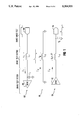
- FIG. 2 shows a system wherein a first preferred embodiment of the present invention is implemented.
- a circuit board 202 to be tested is placed on top of a board test fixture 204 via the guidance of an alignment pin 205.
- the board test fixture 204 provides an electrical interface between the circuit board 202 and the board test system 206. In other words, many test signals travel through the board test fixture 204.
- the present invention envisions implementing a grounding system which utilizes ground coax assemblies 208 and a plated alignment plate 210 in the board test fixture 204, as are described in detail below.
- the grounding system permits testing of the circuit board 202 at very high speeds.
- test signal paths travel from the board test system 206 through the board test fixture 204 to electronic components 212,214 on a circuit board 202 under test.
- a test signal from the board test system 206 travels through the wire-wrapping pin 216 of a personality pin 218, through a wire 220, and then through a signal probe 222, respectively, before reaching the electronic component 212.
- the location of the personality pins and the signal probes as well as the length of their connecting wires changes depending upon the orientation of electronic components 212,214 on the circuit board 202 under test.
- Ground connectors from the board test system 206 contact the bottom of the board test fixture 204 in order to make the ground path available to the fixture 204.
- the alignment plate 210 which serves as a focus means to capture and guide personality pins 218, which carry test signals, into an organized orthogonal array-like pattern when the alignment plate 210 is installed so that the board test system 206 can send test signals through the fixture 204.
- the alignment plate 210 further serves as a ground conductance means. It comprises an inner non-conductive support material 223 and a conductive outer plating 224 on all of its exposed surface areas, including the top, bottom, and through-ways.
- the plating 224 is preferably a metal.
- the metal is a combination of copper and nickel or a combination of copper, nickel, and gold, in order to provide an excellent transitional ground path from the board test system 206 to the top 226 of the alignment plate 210.
- the plated alignment plate 210 provides a good impedance control because it positions the ground path near the signal paths.
- the coax assembly 208 is positioned concentrically around each signal path, specifically each personality pin, which carries a signal posing a potential ground bounce problem.
- signal paths are called "critical" signal paths.
- the critical signal paths are usually those paths which carry electrical signals which switch at a high speed.
- the ground signal carried by the coax assembly 208 is isolated from the internal wire-wrap pin 216 via a piece of plastic tubing 228.
- the plastic tubing 228 extends from the wire wrap at the base of the wire-wrap pin 216 to just short of the tip of the pin 216.
- the plastic tubing 228 extends down through the plated alignment plate 210 in order to prevent the pin 216 from contacting the plating 224, thereby tainting the test signal on pin 216.
- FIGS. 3(a) and 3(b) show in detail the ground coax assembly 208.
- the ground coax assembly comprises a conductive, internal coax sleeve 302, a spring 304, a conductive, external coax sleeve 306, and a plastic insulator 308.
- the sleeve 302 is notched, as shown, so as to permit access of
- the wire wrap would be enclosed by the enlarged region 310.
- the bottom part 312 and the top part 314 of the coax assembly 208 are forced apart by the compression spring 304.
- a stop 316 is designed to catch the external coax sleeve 306 to prevent the coax assembly 208 from coming completely apart.
- the top part 314 of the coax assembly 208 which has sharp edges, is pressed against an internal ground plane 230 mounted inside the board test fixture 204 by the spring 304.
- the bottom part 312 of the coax assembly 208 is forced by the spring 304 against the metal plating 224 of the alignment plate 210 described above.
- the internal ground plane 230 has plating 232 at its underside only and is located near the base of the wire-wrap pin 216.
- the signal wire 220 which passes between the notch at the upper part 314 of the coax assembly 212, is routed in very close proximity to the internal ground plane 230 in order to provide strip line impedance control for the critical signal wire. It should be noted that once the wire 220 leaves the plating 232 of the internal ground plane 230 by more than 1/2 a wire diameter, or so, the impedance adversely rises quickly.
- the ground signal is provided to the circuit board 202 via the various ground probes and various ground pins which are soldered to the plating 232.
- a ground probe 234 is soldered to the plating 232 at a point 236.
- a small ground pin 238 is soldered to the plating 232 at a soldering point 240.
- Both the ground probe 234 and the ground pin 238 carry the ground signal through a probe plate 242 to an external ground plane 244, which is optional.
- the ground probe 234 and the ground pin 238 are soldered to the external ground plane 244 at respective soldering points 246 and 248.
- the ground probe 234 extends further upward in order to contact the ground on the electronic component 214 in a direct manner to make an electrical contact, as shown at reference number 235.
- the external ground plane 244 and the array of small ground pins, such as the ground pin 238, may be conveniently eliminated from the structure. Such a simplified fixture would be cheaper and much easier to construct.
- an insulator such as for example the plastic insulator 308, is provided to surround the corresponding wire-wrap pin so that it does not contact the plating 224 on the alignment plate 210.
- the personality pin 250 is concentrically surrounded along its axis by an insulator 252.
- FIG. 4 illustrates a second preferred embodiment of the present invention.
- the second preferred embodiment is similar to the first preferred embodiment of FIG. 2 in many respects.
- the alignment plate 410 of FIG. 4 does not comprise a conductive outer plating, as does the alignment plate 210 of FIG. 2.
- the alignment plate 410 comprises a ground comb 412, which is a sheet metal part placed, bonded, or affixed in some fashion, onto the alignment plate 410.
- the ground comb 412 is affixed to the alignment plate 410 via a snap-fit arrangement.
- the ground comb 412 comprises one or more protruding parts which snap into the alignment plate 410 to thereby hold the ground comb 412 contiguous to the alignment plate 410.
- the ground comb 412 communicates the ground from the board test system 206 through the alignment plate 410 to any coax assemblies 208.
- the plated alignment plate 210 of FIG. 2 provides slightly better impedance control than the combination of the ground comb 412 and alignment plate 410 of FIG. 4 because it generally provides a ground path more closely coupled to the signal paths.
- the plated alignment plate technique is more expensive than the ground comb technique. Consequently, a cost versus performance analysis must be performed in order to select the best option for a particular embodiment.
- FIG. 5 shows a third preferred embodiment of the present invention wherein an array of ground personality pins 502,504 are implemented in order to control impedance through the board test fixture 204.
- the array of ground personality pins 502,504 are intermixed among the array of test signal personality pins 506.
- the ground personality pins 502,504 can be clustered, if desired, around critical signal paths to more efficiently control impedance.
- ground personality pins 502,504 are mounted in the probe plate 240 and their wire-wrap pins 512,514 are then soldered to the internal ground plane 230, as indicated at reference numerals 522,524.
- the ground personality pins 502,504 are made available to the board test system 206 via an alignment plate 504.
- the alignment plate 510 is essentially composed of a non-conductive plastic material.
- the alignment plate 510 essentially serves as a focus means to capture and guide both the ground personality pins 502,504 and the test signal personality pins 506 into an organized orthogonal array-like pattern when the alignment plate 510 is installed, so that the board test system 206 has easy access to both types of pins at the bottom of the board test fixture 204.
- ground personality pins 502,504 as well as the test signal personality pins 506,508 may bend, as shown by respective wire-wrap pins 512,518 in order to pass through the alignment plate 510 to the board test system 206.
- the metal bodies of the ground personality pins 502,504 may extend out past the top of the probe plate 240, where their top ends may be soldered to the external ground plane 244, thus further controlling impedance.
- FIG. 5 illustrates the ground personality pin 504 with its metal body extended and soldered to the external ground plane 244, as indicated by reference numeral 534.
- the external ground plane 244 is an optional feature of the present invention. If the external ground plane 244 is not needed, the bodies of the ground personality pins 502,504 need only be long enough to press into the probe plate 240. Needless to say, in this case, the bodies of the ground personality pins 502,504 need not be conductive.
- the holes in the internal ground plane 230 for the ground personality pins 502,504 can be sized in order to allow soldering to the internal ground plane 230. If too much hole clearance exists, soldering can be difficult. In contrast, clearance for test signal personality pins 512 need to be great enough to guarantee that the pins 512 will not accidentally touch the plating 232 of the internal ground plane 230. Furthermore, in order to help capture all of the ground personality pins 502,504 at once when the internal ground plane 230 is installed, the small clearance holes in the internal ground plane 220 should be countersunk, as shown.
Abstract
Description
Claims (20)
Priority Applications (3)
| Application Number | Priority Date | Filing Date | Title |
|---|---|---|---|
| US07/741,719 US5304921A (en) | 1991-08-07 | 1991-08-07 | Enhanced grounding system for short-wire lengthed fixture |
| EP92306763A EP0527566A1 (en) | 1991-08-07 | 1992-07-23 | Enhanced grounding system for short-wire lengthed fixture |
| JP4223318A JPH05256905A (en) | 1991-08-07 | 1992-07-30 | Ground system for short-circuit wire test fixture |
Applications Claiming Priority (1)
| Application Number | Priority Date | Filing Date | Title |
|---|---|---|---|
| US07/741,719 US5304921A (en) | 1991-08-07 | 1991-08-07 | Enhanced grounding system for short-wire lengthed fixture |
Publications (1)
| Publication Number | Publication Date |
|---|---|
| US5304921A true US5304921A (en) | 1994-04-19 |
Family
ID=24981882
Family Applications (1)
| Application Number | Title | Priority Date | Filing Date |
|---|---|---|---|
| US07/741,719 Expired - Lifetime US5304921A (en) | 1991-08-07 | 1991-08-07 | Enhanced grounding system for short-wire lengthed fixture |
Country Status (3)
| Country | Link |
|---|---|
| US (1) | US5304921A (en) |
| EP (1) | EP0527566A1 (en) |
| JP (1) | JPH05256905A (en) |
Cited By (8)
| Publication number | Priority date | Publication date | Assignee | Title |
|---|---|---|---|---|
| US5510722A (en) * | 1992-12-18 | 1996-04-23 | Tti Testron, Inc. | Test fixture for printed circuit boards |
| US5633598A (en) * | 1993-06-23 | 1997-05-27 | Everett Charles Technologies, Inc. | Translator fixture with module for expanding test points |
| US5703494A (en) * | 1994-11-09 | 1997-12-30 | Tokyo Electron Limited | Probing test apparatus |
| US20020173072A1 (en) * | 2001-05-18 | 2002-11-21 | Larson Thane M. | Data capture plate for substrate components |
| US6559664B2 (en) | 2001-08-13 | 2003-05-06 | Desimone Peter | Probe plate assembly for a circuit board test fixture |
| US6714034B2 (en) * | 2002-04-11 | 2004-03-30 | Andy Chen | Integrated circuit testing apparatus having stable ground reference |
| US20060103369A1 (en) * | 2004-11-04 | 2006-05-18 | Josef Gluch | Apparatus and method for making ground connection |
| US20070290771A1 (en) * | 2006-06-20 | 2007-12-20 | Qiang Richard Chen | Grounding strategy for filter on planar substrate |
Families Citing this family (2)
| Publication number | Priority date | Publication date | Assignee | Title |
|---|---|---|---|---|
| US5625299A (en) * | 1995-02-03 | 1997-04-29 | Uhling; Thomas F. | Multiple lead analog voltage probe with high signal integrity over a wide band width |
| CN110736914B (en) * | 2019-10-17 | 2022-02-11 | 南宁影联医学工程有限公司 | Detection method of medical equipment interface board |
Citations (19)
| Publication number | Priority date | Publication date | Assignee | Title |
|---|---|---|---|---|
| US3911361A (en) * | 1974-06-28 | 1975-10-07 | Ibm | Coaxial array space transformer |
| US3963986A (en) * | 1975-02-10 | 1976-06-15 | International Business Machines Corporation | Programmable interface contactor structure |
| US4419626A (en) * | 1981-08-25 | 1983-12-06 | Daymarc Corporation | Broad band contactor assembly for testing integrated circuit devices |
| US4544888A (en) * | 1981-11-02 | 1985-10-01 | Joseph Kvaternik | Miniature circuit processing devices and matrix test heads for use therein |
| US4616178A (en) * | 1982-05-27 | 1986-10-07 | Harris Corporation | Pulsed linear integrated circuit tester |
| US4712062A (en) * | 1984-12-20 | 1987-12-08 | Hughes Aircraft Company | Ground shield apparatus for giga-hertz test jig |
| US4731577A (en) * | 1987-03-05 | 1988-03-15 | Logan John K | Coaxial probe card |
| US4739259A (en) * | 1986-08-01 | 1988-04-19 | Tektronix, Inc. | Telescoping pin probe |
| US4740746A (en) * | 1984-11-13 | 1988-04-26 | Tektronix, Inc. | Controlled impedance microcircuit probe |
| US4795977A (en) * | 1987-03-19 | 1989-01-03 | Pacific Western Systems, Inc. | Interface system for interfacing a device tester to a device under test |
| US4799007A (en) * | 1985-11-01 | 1989-01-17 | Hewlett-Packard Company | Bendable pin board test fixture |
| US4894612A (en) * | 1987-08-13 | 1990-01-16 | Hypres, Incorporated | Soft probe for providing high speed on-wafer connections to a circuit |
| US4912401A (en) * | 1989-01-18 | 1990-03-27 | Tektronix, Inc. | Connection apparatus for interactively accessing an electronic device in a pin grid array socket |
| US4973256A (en) * | 1989-08-18 | 1990-11-27 | Texas Instruments Incorporated | Device under test interface board and test electronic card interconnection in semiconductor test system |
| US4996478A (en) * | 1990-01-05 | 1991-02-26 | Tektronix, Inc. | Apparatus for connecting an IC device to a test system |
| US5014002A (en) * | 1989-04-18 | 1991-05-07 | Vlsi Technology, Inc. | ATE jumper programmable interface board |
| US5041782A (en) * | 1989-09-20 | 1991-08-20 | Design Technique International, Inc. | Microstrip probe |
| US5066907A (en) * | 1990-02-06 | 1991-11-19 | Cerprobe Corporation | Probe system for device and circuit testing |
| US5068602A (en) * | 1990-09-07 | 1991-11-26 | Tektronix, Inc. | DUT board for a semiconductor device tester having a reconfigurable coaxial interconnect grid and method of using same |
-
1991
- 1991-08-07 US US07/741,719 patent/US5304921A/en not_active Expired - Lifetime
-
1992
- 1992-07-23 EP EP92306763A patent/EP0527566A1/en not_active Ceased
- 1992-07-30 JP JP4223318A patent/JPH05256905A/en active Pending
Patent Citations (19)
| Publication number | Priority date | Publication date | Assignee | Title |
|---|---|---|---|---|
| US3911361A (en) * | 1974-06-28 | 1975-10-07 | Ibm | Coaxial array space transformer |
| US3963986A (en) * | 1975-02-10 | 1976-06-15 | International Business Machines Corporation | Programmable interface contactor structure |
| US4419626A (en) * | 1981-08-25 | 1983-12-06 | Daymarc Corporation | Broad band contactor assembly for testing integrated circuit devices |
| US4544888A (en) * | 1981-11-02 | 1985-10-01 | Joseph Kvaternik | Miniature circuit processing devices and matrix test heads for use therein |
| US4616178A (en) * | 1982-05-27 | 1986-10-07 | Harris Corporation | Pulsed linear integrated circuit tester |
| US4740746A (en) * | 1984-11-13 | 1988-04-26 | Tektronix, Inc. | Controlled impedance microcircuit probe |
| US4712062A (en) * | 1984-12-20 | 1987-12-08 | Hughes Aircraft Company | Ground shield apparatus for giga-hertz test jig |
| US4799007A (en) * | 1985-11-01 | 1989-01-17 | Hewlett-Packard Company | Bendable pin board test fixture |
| US4739259A (en) * | 1986-08-01 | 1988-04-19 | Tektronix, Inc. | Telescoping pin probe |
| US4731577A (en) * | 1987-03-05 | 1988-03-15 | Logan John K | Coaxial probe card |
| US4795977A (en) * | 1987-03-19 | 1989-01-03 | Pacific Western Systems, Inc. | Interface system for interfacing a device tester to a device under test |
| US4894612A (en) * | 1987-08-13 | 1990-01-16 | Hypres, Incorporated | Soft probe for providing high speed on-wafer connections to a circuit |
| US4912401A (en) * | 1989-01-18 | 1990-03-27 | Tektronix, Inc. | Connection apparatus for interactively accessing an electronic device in a pin grid array socket |
| US5014002A (en) * | 1989-04-18 | 1991-05-07 | Vlsi Technology, Inc. | ATE jumper programmable interface board |
| US4973256A (en) * | 1989-08-18 | 1990-11-27 | Texas Instruments Incorporated | Device under test interface board and test electronic card interconnection in semiconductor test system |
| US5041782A (en) * | 1989-09-20 | 1991-08-20 | Design Technique International, Inc. | Microstrip probe |
| US4996478A (en) * | 1990-01-05 | 1991-02-26 | Tektronix, Inc. | Apparatus for connecting an IC device to a test system |
| US5066907A (en) * | 1990-02-06 | 1991-11-19 | Cerprobe Corporation | Probe system for device and circuit testing |
| US5068602A (en) * | 1990-09-07 | 1991-11-26 | Tektronix, Inc. | DUT board for a semiconductor device tester having a reconfigurable coaxial interconnect grid and method of using same |
Cited By (11)
| Publication number | Priority date | Publication date | Assignee | Title |
|---|---|---|---|---|
| US5510722A (en) * | 1992-12-18 | 1996-04-23 | Tti Testron, Inc. | Test fixture for printed circuit boards |
| US5633598A (en) * | 1993-06-23 | 1997-05-27 | Everett Charles Technologies, Inc. | Translator fixture with module for expanding test points |
| US5798654A (en) * | 1993-06-23 | 1998-08-25 | Everett Charles Technologies, Inc. | Translator fixture with module for expanding test points |
| US5703494A (en) * | 1994-11-09 | 1997-12-30 | Tokyo Electron Limited | Probing test apparatus |
| US20020173072A1 (en) * | 2001-05-18 | 2002-11-21 | Larson Thane M. | Data capture plate for substrate components |
| US6559664B2 (en) | 2001-08-13 | 2003-05-06 | Desimone Peter | Probe plate assembly for a circuit board test fixture |
| US6714034B2 (en) * | 2002-04-11 | 2004-03-30 | Andy Chen | Integrated circuit testing apparatus having stable ground reference |
| US20060103369A1 (en) * | 2004-11-04 | 2006-05-18 | Josef Gluch | Apparatus and method for making ground connection |
| US7161365B2 (en) | 2004-11-04 | 2007-01-09 | Infineon Technologies Ag | Apparatus and method for making ground connection |
| US20070290771A1 (en) * | 2006-06-20 | 2007-12-20 | Qiang Richard Chen | Grounding strategy for filter on planar substrate |
| US7532092B2 (en) | 2006-06-20 | 2009-05-12 | Tdk Corporation | Grounding strategy for filter on planar substrate |
Also Published As
| Publication number | Publication date |
|---|---|
| JPH05256905A (en) | 1993-10-08 |
| EP0527566A1 (en) | 1993-02-17 |
Similar Documents
| Publication | Publication Date | Title |
|---|---|---|
| EP0702797B1 (en) | Integrated circuit probing apparatus including a capacitor bypass structure | |
| US6603322B1 (en) | Probe card for high speed testing | |
| US4891585A (en) | Multiple lead probe for integrated circuits in wafer form | |
| US4764723A (en) | Wafer probe | |
| JPS6138191Y2 (en) | ||
| US5014002A (en) | ATE jumper programmable interface board | |
| KR100745104B1 (en) | Contactor probe, electric probe unit, combination of a probe assembly and a insulator for contactor probe, and elastic conductive probe assembly | |
| US6323667B1 (en) | Contact probe unit | |
| US5304921A (en) | Enhanced grounding system for short-wire lengthed fixture | |
| US6203329B1 (en) | Impedance controlled interconnection device | |
| EP0163211A2 (en) | High density probe-head with isolated and shielded transmission lines | |
| US4764722A (en) | Coaxial probe | |
| JPS5932740B2 (en) | Coaxial array space converter | |
| US4956604A (en) | Broad band contactor assembly for testing integrated circuit devices | |
| US5283518A (en) | Method for the control of ground bounce below an internal ground plane in a short-wire board test fixture | |
| EP0298219A2 (en) | Method and apparatus for testing unpackaged integrated circuits in a hybrid circuit environment | |
| US5389874A (en) | Method for control of ground bounce above an internal ground plane in a short-wire board test fixture | |
| JPS62182678A (en) | Test sight system | |
| JP2002506211A (en) | Coaxial probe interface for automatic test equipment | |
| US7230835B1 (en) | Apparatus for reducing signal reflection in a circuit board | |
| US6329892B1 (en) | Low profile, current-driven relay for integrated circuit tester | |
| US6559664B2 (en) | Probe plate assembly for a circuit board test fixture | |
| US3525937A (en) | Matched impedance test probe fixture | |
| JPS5856436B2 (en) | Test equipment for integrated circuit devices | |
| KR200182523Y1 (en) | Probing device |
Legal Events
| Date | Code | Title | Description |
|---|---|---|---|
| AS | Assignment |
Owner name: HEWLETT-PACKARD COMPANY, CALIFORNIA Free format text: ASSIGNMENT OF ASSIGNORS INTEREST.;ASSIGNORS:COOK, STEPHEN J.;KERSCHNER, RONALD K.;REEL/FRAME:005953/0741 Effective date: 19910805 |
|
| STCF | Information on status: patent grant |
Free format text: PATENTED CASE |
|
| FEPP | Fee payment procedure |
Free format text: PAYOR NUMBER ASSIGNED (ORIGINAL EVENT CODE: ASPN); ENTITY STATUS OF PATENT OWNER: LARGE ENTITY |
|
| FPAY | Fee payment |
Year of fee payment: 4 |
|
| AS | Assignment |
Owner name: HEWLETT-PACKARD COMPANY, A DELAWARE CORPORATION, C Free format text: MERGER;ASSIGNOR:HEWLETT-PACKARD COMPANY, A CALIFORNIA CORPORATION;REEL/FRAME:010841/0649 Effective date: 19980520 |
|
| AS | Assignment |
Owner name: AGILENT TECHNOLOGIES INC, CALIFORNIA Free format text: ASSIGNMENT OF ASSIGNORS INTEREST;ASSIGNOR:HEWLETT-PACKARD COMPANY;REEL/FRAME:010977/0540 Effective date: 19991101 |
|
| FPAY | Fee payment |
Year of fee payment: 8 |
|
| FPAY | Fee payment |
Year of fee payment: 12 |