US20100034026A1 - Erase method and non-volatile semiconductor memory - Google Patents
Erase method and non-volatile semiconductor memory Download PDFInfo
- Publication number
- US20100034026A1 US20100034026A1 US12/535,903 US53590309A US2010034026A1 US 20100034026 A1 US20100034026 A1 US 20100034026A1 US 53590309 A US53590309 A US 53590309A US 2010034026 A1 US2010034026 A1 US 2010034026A1
- Authority
- US
- United States
- Prior art keywords
- erase
- unit
- units
- verification
- fail
- Prior art date
- Legal status (The legal status is an assumption and is not a legal conclusion. Google has not performed a legal analysis and makes no representation as to the accuracy of the status listed.)
- Granted
Links
- 238000000034 method Methods 0.000 title claims abstract description 31
- 239000004065 semiconductor Substances 0.000 title claims description 6
- 238000012795 verification Methods 0.000 claims abstract description 62
- 239000000758 substrate Substances 0.000 claims description 3
- 238000013459 approach Methods 0.000 description 4
- 238000004519 manufacturing process Methods 0.000 description 4
- 230000001143 conditioned effect Effects 0.000 description 3
- 239000002131 composite material Substances 0.000 description 2
- 239000000470 constituent Substances 0.000 description 2
- 238000007796 conventional method Methods 0.000 description 2
- 238000012986 modification Methods 0.000 description 2
- 230000004048 modification Effects 0.000 description 2
- 230000001629 suppression Effects 0.000 description 2
- 230000004075 alteration Effects 0.000 description 1
- 230000003247 decreasing effect Effects 0.000 description 1
- 230000000694 effects Effects 0.000 description 1
- 238000010348 incorporation Methods 0.000 description 1
- 239000000463 material Substances 0.000 description 1
- 102220124522 rs746215581 Human genes 0.000 description 1
- 230000005641 tunneling Effects 0.000 description 1
Images


Classifications
-
- G—PHYSICS
- G11—INFORMATION STORAGE
- G11C—STATIC STORES
- G11C16/00—Erasable programmable read-only memories
- G11C16/02—Erasable programmable read-only memories electrically programmable
- G11C16/06—Auxiliary circuits, e.g. for writing into memory
- G11C16/34—Determination of programming status, e.g. threshold voltage, overprogramming or underprogramming, retention
- G11C16/3436—Arrangements for verifying correct programming or erasure
- G11C16/344—Arrangements for verifying correct erasure or for detecting overerased cells
-
- G—PHYSICS
- G11—INFORMATION STORAGE
- G11C—STATIC STORES
- G11C16/00—Erasable programmable read-only memories
- G11C16/02—Erasable programmable read-only memories electrically programmable
- G11C16/06—Auxiliary circuits, e.g. for writing into memory
- G11C16/10—Programming or data input circuits
- G11C16/14—Circuits for erasing electrically, e.g. erase voltage switching circuits
- G11C16/16—Circuits for erasing electrically, e.g. erase voltage switching circuits for erasing blocks, e.g. arrays, words, groups
Definitions
- the present disclosure relates to an erase method for non-volatile semiconductor memory devices. More particularly, the disclosure relates to an erase method for NOR flash memory devices.
- NOR flash memory is a well known type of non-volatile memory capable of retaining stored data in the absence of applied power, yet also capable of being electrically erasable and electrically programmable.
- One conventional approach to the implementation of an erase method for nonvolatile memory is disclosed, for example, in Japan Patent Publication Nos. 2000-348492 and H8-77782. The conventional approach variously describes a block erase mode, a multi block erase mode, and a chip erase mode.
- An erase operation performed by a NOR flash memory is typically conducted on the basis of a defined “erase unit”, (i.e., a memory block size capable of being erased during a single erase operation).
- a defined “erase unit” i.e., a memory block size capable of being erased during a single erase operation.
- Emerging NOR flash memory devices are characterized by an increasing erase unit size. That is, where previous NOR flash memory had an erase unit of 0.5 M, emerging NOR flash memory has an erase unit of 2.0 M. This expansion of erase unit size follows an increase in the number of NOR flash memory devices incorporating multi level memory cells (MLCs). The incorporation of MLCs allows contemporary NOR flash memory to store more data per unit area of constituent chip size.
- MLCs multi level memory cells
- the number of physical memory cells conditioned by an erase operation must be increased.
- the number of inner physical memory cells should be 1.0 M which is twice the conventional number of memory cells.
- FIG. 5 graphically illustrates this phenomenon. The results illustrated in FIG. 5 occur immediately after an erase operation is completed, but before “treatment” of the memory cells which is typical in erase operations for flash memory.
- the 1.0 M memory cells may be erased as two (2) 0.5 M memory cell units connected in series.
- the use of conventional suppression techniques becomes possible with an erase threshold voltage distribution width typical for 0.5 M memory cells.
- a conventionally similar erase operation may be used for each of the two 0.5 M memory cell units, potential alteration of the fabrication process is not required.
- Embodiments of the invention provide an erase method for a non-volatile semiconductor memory device in which erase threshold voltage distribution for the constituent memory cells is similar to that of much smaller erase units (e.g., 0.5 M memory cells), yet without an material expansion in the amount of time required to perform an erase operation.
- erase threshold voltage distribution for the constituent memory cells is similar to that of much smaller erase units (e.g., 0.5 M memory cells), yet without an material expansion in the amount of time required to perform an erase operation.
- Embodiments of the invention provide an erase method for a non-volatile memory device having a defined erase unit divided into first and second inner erase units, the method comprising; applying an erase voltage to at least one of the first and second inner erase units in accordance with respective states of corresponding first and second fail flags, after applying the erase voltage to the at least one of the first and second inner erase units, performing an erase verification on the at least one of the first and second inner erase units, and updating the at least one of the first and second fail flags in accordance with erase verification results.
- Embodiments of the invention also provide a non-volatile memory device, comprising; an array of memory cell arranged in a plurality of erase unit blocks according to a defined erase unit, wherein each one of the plurality of erase unit blocks is divided into first and second inner erase units, a first well region containing the memory cells corresponding to the first inner erase unit and a second well region containing the memory cells corresponding to the second inner erase unit, wherein the first and second well regions are electrically separated on a semiconductor substrate.
- Embodiments of the invention also provide a non-volatile memory device, comprising; an array of memory cell arranged in a plurality of erase unit blocks according to a defined erase unit, wherein each one of the plurality of erase unit blocks is divided into first and second inner erase units, a common well region containing the memory cells corresponding to the first and second inner erase units, a first group of word lines corresponding to the memory cells of the first inner erase unit arranged on the well region, and a second group of word lines corresponding to the memory cells of the second inner erase unit arranged on the well region, wherein the first and second word lines are configured for independent application of a bias voltage during an erase operation, such that the first and second inner erase units may be erased and erased verified during the erase operation.
- FIG. 1 is a flowchart summarizing an erase method according to an embodiment of the invention
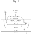
- FIG. 2 is a sectional view of a flash memory cell and its voltage bias conditions during an erase operation
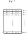
- FIG. 3 is a conceptual view of a memory cell array structure for a NOR flash memory incorporating the flash memory cell of FIG. 2 ;
- FIG. 4 is a partial plan view of a memory cell array to which an erase method according to an embodiment of the invention is applied.
- FIG. 5 illustrates threshold voltage distribution characteristics for memory cells.
- FIG. 2 is a sectional structure of a flash memory cell as biased during an erase operation according to an embodiment of the invention.
- the flash memory cell comprises; an N-well 12 and a P-well 13 successively are formed in a P-type substrate 11 .
- Source/drain regions 14 for the flash memory cell are formed in the P-well 13 .
- a floating gate 15 and a control gate 16 are stacked on the P-well 13 between the source/drain regions 14 .
- the control gate 16 is connected to a word line WL.
- NOR flash memory cell having the above structure, a negative voltage Vneg ( ⁇ 9V) is applied from a charge pump to the word line WL during an erase operation, and a positive voltage Vpm ( ⁇ +9V) is applied from another charge pump to the well regions 12 and 13 .
- Vneg ⁇ 9V
- Vpm ⁇ +9V
- FN tunneling a well understood phenomenon
- data is erased from the NOR flash memory cell.
- a reference voltage greater than the threshold voltage of the erased cell is applied to the word line WL to essentially perform a read operation. By means of this read operation it is determined whether or not the erase operation has been successfully performed. If the erase verification fails, then the erase operation is repeated.
- FIG. 3 is a conceptual plan view of a memory cell array for a NOR flash memory including a plurality of the above-mentioned flash memory cells.
- the memory cell array includes a plurality of word lines, a plurality of bit lines, and the plurality of memory cells connected thereto.
- FIG. 3 is a conceptual plan view of a memory cell array for a NOR flash memory including a plurality of the above-mentioned flash memory cells.
- the memory cell array includes a plurality of word lines, a plurality of bit lines, and the plurality of memory cells connected thereto.
- the memory cell array is operationally divided into (e.g.,) 256 units in relation to an arbitrarily determined “block erase unit.” However, this block erase unit is further divided according to a smaller “inner erase unit.”
- a NOR flash memory implemented in accordance with an embodiment of the invention might internally realize the 1.0 M black erase unit in two inner erase units (e.g., unit A and unit B), wherein each inner erase unit is 0.5 M memory cells.
- the following erase method may be used during an erase operation.
- FIG. 1 is a flowchart summarizing in one embodiment of the invention the above-described approach.
- treatment of the memory cells before erase may be performed (S 1 ). Fail flags are then initialized (reset) in the memory unit (S 2 ).
- S 1 treatment of the memory cells before erase
- Fail flags are then initialized (reset) in the memory unit (S 2 ).
- a current erase unit e.g., BLK 0 in FIG. 3
- second inner erase unit (B) S 7
- a composite verification determination is made for both the first and second inner erase units (A and B) (S 10 ).
- Every inner erase unit e.g., A and B
- the current erase unit e.g., BLK 0
- the treatment of the memory cells post erasure S 11 may be performed, before the erase operation is completed.
- the erase operation returns to the application of the erase voltage (S 3 ), and the erase/verification loop continues.
- FIG. 1 The embodiment of the invention illustrated in FIG. 1 provides the following:
- each inner erase unit A or B
- Each successively applied erase voltage may be modified (i.e., increased) over the previous erase/verification loop.
- conventionally similar erase/verification techniques may be used despite a larger defined erase unit size. For example, again returning to the emerging 1.0 M memory cells requirement verses the 0.5 M memory cells convention, the same type of read operation may be used during the erase verification step as have been applied to the 0.5 M memory cells convention with similar effects of erase threshold voltage distribution.
- the erase voltage may be simultaneously applied to respective inner erase units within multiple erase units (e.g., BLK 0 through BLK 255 of FIG. 3 ) it is possible to erase multiple erase blocks, each having a (2 ⁇ ) expanded erase unit size, in about the same time as was conventionally required.
- an erase method that further divides a defined erase unit into a plurality of inner erase units for controlling application of an erase voltage allows; (a) each well region containing a memory cell array for each erase unit to be separated and independently controlled, (b) each well region containing a memory cell array is shared, but a word line may be separately controlled for each erase unit, and (c) each well region containing a memory cell array may be separated by an erase unit and independently controlled, and a word line is independently controlled by an erase unit.
- FIG. 4 is a plan view further illustrating a method of separating an erase unit into a plurality of inner erase units according to an embodiment of the invention.
- This example again assumes an erase unit of about 1.0 M memory cells.
- a common P-well region is used for each one of the inner erase units forming the larger erase unit.
- Four dummy word lines D 1 to D 4 are disposed between adjacent P-well regions along a horizontal (or row, or word line) axis.
- a first group (WL 1 ) of 256 word lines corresponding to the first (unit A) inner erase unit is disposed to one side of (e.g., “above”) the dummy word lines.
- a second group (WL 2 ) of 256 word lines corresponding to the second (unit B) inner erase unit is disposed to the other side of the dummy word lines. Additionally, bounded by the dummy word lines D 1 to D 4 , a first group (BL 1 ) of 2048 bit lines corresponding to the first (unit A) inner erase unit extends across the corresponding P-well region, and a second group (BL 2 ) of 2048 bit lines corresponding to the second (unit B) inner erase unit extends across the other corresponding P-well region.
- a common P-well region may be used, but corresponding word line voltages will be independently controlled during an erase operation.
- Embodiments of the invention have been described in the context of a NOR flash memory, but other embodiments of the invention encompass NAND flash memory.
- an erase unit structure and corresponding erase/verification method may be adopted to deal with an expanded erase unit size, without the need of changing the manufacturing processes for the device. Nonetheless, erase threshold voltage distribution and erase time can remain almost the same as for devices defining a smaller erase unit size.
Abstract
Description
- This U.S. non-provisional patent application claims priority under 35 U.S.C. §119 to Japanese Patent Application No. 10-2008-203422 filed on Aug. 6, 2008, and to Korean Patent Application No. 10-2009-0068260 filed on Jul. 27, 2009, the subject matter of which are hereby incorporated by reference.
- The present disclosure relates to an erase method for non-volatile semiconductor memory devices. More particularly, the disclosure relates to an erase method for NOR flash memory devices.
- NOR flash memory is a well known type of non-volatile memory capable of retaining stored data in the absence of applied power, yet also capable of being electrically erasable and electrically programmable. One conventional approach to the implementation of an erase method for nonvolatile memory is disclosed, for example, in Japan Patent Publication Nos. 2000-348492 and H8-77782. The conventional approach variously describes a block erase mode, a multi block erase mode, and a chip erase mode.
- An erase operation performed by a NOR flash memory is typically conducted on the basis of a defined “erase unit”, (i.e., a memory block size capable of being erased during a single erase operation). Emerging NOR flash memory devices are characterized by an increasing erase unit size. That is, where previous NOR flash memory had an erase unit of 0.5 M, emerging NOR flash memory has an erase unit of 2.0 M. This expansion of erase unit size follows an increase in the number of NOR flash memory devices incorporating multi level memory cells (MLCs). The incorporation of MLCs allows contemporary NOR flash memory to store more data per unit area of constituent chip size.
- To accommodate an increasing erase unit size for NOR flash memory incorporating MLCs, the number of physical memory cells conditioned by an erase operation must be increased. For example, in order to realize an erase unit of 2.0 M in a NOR flash memory incorporating MLCs, the number of inner physical memory cells should be 1.0 M which is twice the conventional number of memory cells.
- However, increasing the number of physical memory cells conditioned by an erase operation raises some difficult issues. Some of these issues will now be described using an assumption that the number of physical memory cells being conditioned in 1.0 M. First, because the number of physical memory cells is now double that of previous conventional NOR flash memory devices, the threshold voltage distribution (Vt distribution) for the 1.0 M memory cells may broaden following completion of an erase operation, as compared with the threshold voltage distribution for 0.5 M memory cells. Figure (FIG.) 5 graphically illustrates this phenomenon. The results illustrated in
FIG. 5 occur immediately after an erase operation is completed, but before “treatment” of the memory cells which is typical in erase operations for flash memory. - As is conventionally understood, it is necessary to prevent an over-erase condition for memory cells in NOR flash memory. Once the threshold voltage distribution has broadened, it is necessary to suppress the incidence rate of over-erase by raising the reference voltage used during erase verification. However, this means that the upper limit of the threshold voltage for an erased memory cell must be increased, thereby decreasing read margin for the memory cell.
- Thus, in order to realize an erase threshold voltage distribution similar to that previously obtained for 0.5 M memory cells, an erase operation applied to 1.0 M memory cells must carefully consider the erase verification process and possibly adjustments to the memory cell fabrication process. Further, the prompt application of certain conventional suppression techniques becomes complicated.
- It is further assumed, consistent with conventional practice, that the 1.0 M memory cells may be erased as two (2) 0.5 M memory cell units connected in series. In such a case, the use of conventional suppression techniques becomes possible with an erase threshold voltage distribution width typical for 0.5 M memory cells. Furthermore, since a conventionally similar erase operation may be used for each of the two 0.5 M memory cell units, potential alteration of the fabrication process is not required.
- However, the serial erasure of two 0.5 M memory cell units unduly extends the time required to erase the entire 1.0 M memory cells using conventional techniques.
- Embodiments of the invention provide an erase method for a non-volatile semiconductor memory device in which erase threshold voltage distribution for the constituent memory cells is similar to that of much smaller erase units (e.g., 0.5 M memory cells), yet without an material expansion in the amount of time required to perform an erase operation.
- Embodiments of the invention provide an erase method for a non-volatile memory device having a defined erase unit divided into first and second inner erase units, the method comprising; applying an erase voltage to at least one of the first and second inner erase units in accordance with respective states of corresponding first and second fail flags, after applying the erase voltage to the at least one of the first and second inner erase units, performing an erase verification on the at least one of the first and second inner erase units, and updating the at least one of the first and second fail flags in accordance with erase verification results.
- Embodiments of the invention also provide a non-volatile memory device, comprising; an array of memory cell arranged in a plurality of erase unit blocks according to a defined erase unit, wherein each one of the plurality of erase unit blocks is divided into first and second inner erase units, a first well region containing the memory cells corresponding to the first inner erase unit and a second well region containing the memory cells corresponding to the second inner erase unit, wherein the first and second well regions are electrically separated on a semiconductor substrate.
- Embodiments of the invention also provide a non-volatile memory device, comprising; an array of memory cell arranged in a plurality of erase unit blocks according to a defined erase unit, wherein each one of the plurality of erase unit blocks is divided into first and second inner erase units, a common well region containing the memory cells corresponding to the first and second inner erase units, a first group of word lines corresponding to the memory cells of the first inner erase unit arranged on the well region, and a second group of word lines corresponding to the memory cells of the second inner erase unit arranged on the well region, wherein the first and second word lines are configured for independent application of a bias voltage during an erase operation, such that the first and second inner erase units may be erased and erased verified during the erase operation.
- The accompanying drawings illustrated certain embodiments of the present invention. In the figures:
-
FIG. 1 is a flowchart summarizing an erase method according to an embodiment of the invention; -
FIG. 2 is a sectional view of a flash memory cell and its voltage bias conditions during an erase operation; -
FIG. 3 is a conceptual view of a memory cell array structure for a NOR flash memory incorporating the flash memory cell ofFIG. 2 ; -
FIG. 4 is a partial plan view of a memory cell array to which an erase method according to an embodiment of the invention is applied; and -
FIG. 5 illustrates threshold voltage distribution characteristics for memory cells. - Hereinafter, exemplary embodiments of the present invention will be described in some additional detail with reference to the accompanying drawings.
-
FIG. 2 is a sectional structure of a flash memory cell as biased during an erase operation according to an embodiment of the invention. The flash memory cell comprises; an N-well 12 and a P-well 13 successively are formed in a P-type substrate 11. Source/drain regions 14 for the flash memory cell are formed in the P-well 13. Moreover, afloating gate 15 and acontrol gate 16 are stacked on the P-well 13 between the source/drain regions 14. Thecontrol gate 16 is connected to a word line WL. - In a NOR flash memory cell having the above structure, a negative voltage Vneg (˜−9V) is applied from a charge pump to the word line WL during an erase operation, and a positive voltage Vpm (˜+9V) is applied from another charge pump to the
well regions floating gate 15 migrate to thewell regions -
FIG. 3 is a conceptual plan view of a memory cell array for a NOR flash memory including a plurality of the above-mentioned flash memory cells. As is conventionally understood, the memory cell array includes a plurality of word lines, a plurality of bit lines, and the plurality of memory cells connected thereto. In the illustrated example ofFIG. 3 , the memory cell array is operationally divided into (e.g.,) 256 units in relation to an arbitrarily determined “block erase unit.” However, this block erase unit is further divided according to a smaller “inner erase unit.” Returning to the example of a defined block erase unit of 1.0 M memory cells, a NOR flash memory implemented in accordance with an embodiment of the invention might internally realize the 1.0 M black erase unit in two inner erase units (e.g., unit A and unit B), wherein each inner erase unit is 0.5 M memory cells. - Moreover, consistent with the illustrated embodiment of the present invention shown in
FIG. 3 , the following erase method may be used during an erase operation. - (1) An erase voltage is simultaneously applied to first (unit A) and second (unit B) inner erase units.
- (2) Erase verification is then performed in series for each erase unit.
- (3) Once an erase verification failure is detected in a first (unit A) inner erase unit, the ongoing erase verification for said inner erase unit is halted, a flag indicating an erase verification fail is stored in a corresponding memory unit, and the erase verification for a corresponding second (unit B) inner erase unit is begun.
- (4) Thus, erase verification for the second (unit B) inner erase unit is performed. If an erase verification failure is detected, the erase verification is halted, and a flag indicating the erase verification failure is stored in the memory unit.
- (5) Since the erase verifications for both inner erase units have failed, a defined erase voltage is applied to both inner erase units based on the stored fail flags.
- (6) The foregoing erase verification steps are repeated, and
-
- (a) during this repetition, if the erase verification for the first (unit A) inner erase unit fails at a certain point and thereafter the erase verification for the second (unit B) inner erase unit passes, a defined erase voltage is applied to only the first (unit A) inner erase unit, or
- (b) during this repetition, if the erase verification for the first (unit A) inner erase unit passes at a certain point and thereafter the erase verification for the second (unit B) inner erase unit fails, a defined erase voltage is applied to only the second (unit B) inner erase unit.
- (7) This approach continues until erase verifications for both inner erase units of each erase unit pass. However, passed erase units (having passed first and second inner erase units) are skipped during subsequent erase verification steps.
-
FIG. 1 is a flowchart summarizing in one embodiment of the invention the above-described approach. Using conventional techniques, treatment of the memory cells before erase may be performed (S1). Fail flags are then initialized (reset) in the memory unit (S2). In the illustrated example, two (2) inner erase units are assumed and corresponding fail flags are reset to A=1 and B=1 in the memory unit. - An erase/verification loop now begins with the fail flag conditional application of an erase voltage to one or both of the inner erase units for a current erase unit (e.g.,
BLK 0 inFIG. 3 ) (S3). Since A=1 and B=1 in the initialization state (S2), the erase voltage is applied to both first and second inner units (A and B) and a corresponding erase operation is performed. - A verification determination is now made for the first inner erase unit (A) (S4). If the corresponding “first” fail flag is reset (A=1) (S4=yes), then the first fail flag is set (A=0) in the memory unit and an erase verification is performed for the first inner erase unit (A) (S5). The fail flag set and erase verification may be performed in parallel.
- If the first inner erase unit (A) passes erase verification (S6=yes), then a verification determination is made for the second inner erase unit (B) (S7). However, if the first inner erase unit (A) fails erase verification, the first fail flag is again reset (A=1) (S12), before performing the verification determination for the second inner erase unit (B) (S7).
- Here again the verification determination relative to the second inner erase unit (B) is made in view of a corresponding “second” fail flag status. If the second fail flag is reset (A=1) (S7=yes), then the second fail flag is set (B=0) in the memory unit and an erase verification is performed for the second inner erase unit (B) (S8). Again, the fail flag set and erase verification may be performed in parallel.
- If the second inner erase unit (A) passes erase verification (S9=yes), then a composite verification determination is made for both the first and second inner erase units (A and B) (S10). However, if the second inner erase unit (B) fails erase verification, the second fail flag is again reset (B=1) (S13), before performing the composite verification determination (S10).
- If every inner erase unit (e.g., A and B) for the current erase unit (e.g., BLK 0) has passed erase verification (S10=yes), the treatment of the memory cells post erasure (S11) may be performed, before the erase operation is completed.
- However, where one or more of the inner erase unit (A and/or B) has not passed verification, the erase operation returns to the application of the erase voltage (S3), and the erase/verification loop continues.
- Where a set fail flag for an inner erase unit (A=0 or B=0) indicates that the corresponding inner erase unit has passed (S4=no or S7=no), a corresponding verification step is omitted.
- The embodiment of the invention illustrated in
FIG. 1 provides the following: - (1) An erase verification is performed on each inner erase unit (A or B) in accordance with the value of a corresponding fail flag result. Each successively applied erase voltage may be modified (i.e., increased) over the previous erase/verification loop. Thus, conventionally similar erase/verification techniques may be used despite a larger defined erase unit size. For example, again returning to the emerging 1.0 M memory cells requirement verses the 0.5 M memory cells convention, the same type of read operation may be used during the erase verification step as have been applied to the 0.5 M memory cells convention with similar effects of erase threshold voltage distribution.
- (2) Since the erase voltage may be simultaneously applied to respective inner erase units within multiple erase units (e.g.,
BLK 0 throughBLK 255 ofFIG. 3 ) it is possible to erase multiple erase blocks, each having a (2×) expanded erase unit size, in about the same time as was conventionally required. - (3) Since the foregoing method uses similar erase/verification techniques as compared with conventional NOR flash memory devices, current manufacturing processes are applicable without modification.
- In addition, an erase method that further divides a defined erase unit into a plurality of inner erase units for controlling application of an erase voltage allows; (a) each well region containing a memory cell array for each erase unit to be separated and independently controlled, (b) each well region containing a memory cell array is shared, but a word line may be separately controlled for each erase unit, and (c) each well region containing a memory cell array may be separated by an erase unit and independently controlled, and a word line is independently controlled by an erase unit.
-
FIG. 4 is a plan view further illustrating a method of separating an erase unit into a plurality of inner erase units according to an embodiment of the invention. This example again assumes an erase unit of about 1.0 M memory cells. Consistent withFIG. 2 , a common P-well region is used for each one of the inner erase units forming the larger erase unit. Four dummy word lines D1 to D4 are disposed between adjacent P-well regions along a horizontal (or row, or word line) axis. Using the dummy word lines D1 to D4 as a boundary, a first group (WL1) of 256 word lines corresponding to the first (unit A) inner erase unit is disposed to one side of (e.g., “above”) the dummy word lines. A second group (WL2) of 256 word lines corresponding to the second (unit B) inner erase unit is disposed to the other side of the dummy word lines. Additionally, bounded by the dummy word lines D1 to D4, a first group (BL1) of 2048 bit lines corresponding to the first (unit A) inner erase unit extends across the corresponding P-well region, and a second group (BL2) of 2048 bit lines corresponding to the second (unit B) inner erase unit extends across the other corresponding P-well region. - Instead of independently controlled, electrically separated P-well regions for the respective inner erase units, a common P-well region may be used, but corresponding word line voltages will be independently controlled during an erase operation.
- Embodiments of the invention have been described in the context of a NOR flash memory, but other embodiments of the invention encompass NAND flash memory.
- According to the foregoing erase methods for non-volatile semiconductor memory devices, an erase unit structure and corresponding erase/verification method may be adopted to deal with an expanded erase unit size, without the need of changing the manufacturing processes for the device. Nonetheless, erase threshold voltage distribution and erase time can remain almost the same as for devices defining a smaller erase unit size.
- The above-disclosed subject matter is to be considered illustrative, and not restrictive, and the appended claims are intended to cover all such modifications, enhancements, and other embodiments, which fall within the scope of the present invention. Thus, to the maximum extent allowed by law, the scope of the present invention is to be determined by the broadest permissible interpretation of the following claims and their equivalents, and shall not be restricted or limited by the foregoing detailed description.
Claims (12)
Applications Claiming Priority (4)
| Application Number | Priority Date | Filing Date | Title |
|---|---|---|---|
| JP2008-203422 | 2008-08-06 | ||
| JP2008203422A JP2010040125A (en) | 2008-08-06 | 2008-08-06 | Erasing method in nonvolatile semiconductor memory device |
| KR10-2009-0068260 | 2009-07-27 | ||
| KR1020090068260A KR20100018457A (en) | 2008-08-06 | 2009-07-27 | Erasing method of non-volatile semiconductor memory device |
Publications (2)
| Publication Number | Publication Date |
|---|---|
| US20100034026A1 true US20100034026A1 (en) | 2010-02-11 |
| US8264891B2 US8264891B2 (en) | 2012-09-11 |
Family
ID=41652818
Family Applications (1)
| Application Number | Title | Priority Date | Filing Date |
|---|---|---|---|
| US12/535,903 Active 2030-09-17 US8264891B2 (en) | 2008-08-06 | 2009-08-05 | Erase method and non-volatile semiconductor memory |
Country Status (1)
| Country | Link |
|---|---|
| US (1) | US8264891B2 (en) |
Cited By (3)
| Publication number | Priority date | Publication date | Assignee | Title |
|---|---|---|---|---|
| TWI501242B (en) * | 2013-10-04 | 2015-09-21 | Winbond Electronics Corp | Erase method for flash |
| US9928916B2 (en) | 2012-09-06 | 2018-03-27 | Toshiba Memory Corporation | Semiconductor memory device |
| US11081196B2 (en) * | 2019-12-05 | 2021-08-03 | Sandisk Technologies Llc | Non-volatile memory with erase verify skip |
Citations (6)
| Publication number | Priority date | Publication date | Assignee | Title |
|---|---|---|---|---|
| US5297148A (en) * | 1989-04-13 | 1994-03-22 | Sundisk Corporation | Flash eeprom system |
| US5509018A (en) * | 1992-09-11 | 1996-04-16 | International Business Machines Corporation | Flash-erase-type nonvolatile semiconductor storage device |
| US6870771B2 (en) * | 2001-08-28 | 2005-03-22 | Renesas Technology Corp. | Nonvolatile semiconductor memory device that can suppress effect of threshold voltage variation of memory cell transistor |
| US7001808B2 (en) * | 2001-08-31 | 2006-02-21 | Renesas Technology Corp. | Semiconductor integrated circuit device having a dummy conductive film and method of manufacturing the same |
| US20080007999A1 (en) * | 2006-07-10 | 2008-01-10 | Park Ki-Tae | Nonvolatile memory device with NAND cell strings |
| US7872917B2 (en) * | 2007-12-25 | 2011-01-18 | Samsung Electronics Co., Ltd. | Non-volatile semiconductor memory device and memory system including the same |
Family Cites Families (2)
| Publication number | Priority date | Publication date | Assignee | Title |
|---|---|---|---|---|
| KR970005644B1 (en) | 1994-09-03 | 1997-04-18 | 삼성전자 주식회사 | Multi-block erase and verify device and method of non-volatile semiconductor memory device |
| JP3920501B2 (en) | 1999-04-02 | 2007-05-30 | 株式会社東芝 | Nonvolatile semiconductor memory device and data erase control method thereof |
-
2009
- 2009-08-05 US US12/535,903 patent/US8264891B2/en active Active
Patent Citations (6)
| Publication number | Priority date | Publication date | Assignee | Title |
|---|---|---|---|---|
| US5297148A (en) * | 1989-04-13 | 1994-03-22 | Sundisk Corporation | Flash eeprom system |
| US5509018A (en) * | 1992-09-11 | 1996-04-16 | International Business Machines Corporation | Flash-erase-type nonvolatile semiconductor storage device |
| US6870771B2 (en) * | 2001-08-28 | 2005-03-22 | Renesas Technology Corp. | Nonvolatile semiconductor memory device that can suppress effect of threshold voltage variation of memory cell transistor |
| US7001808B2 (en) * | 2001-08-31 | 2006-02-21 | Renesas Technology Corp. | Semiconductor integrated circuit device having a dummy conductive film and method of manufacturing the same |
| US20080007999A1 (en) * | 2006-07-10 | 2008-01-10 | Park Ki-Tae | Nonvolatile memory device with NAND cell strings |
| US7872917B2 (en) * | 2007-12-25 | 2011-01-18 | Samsung Electronics Co., Ltd. | Non-volatile semiconductor memory device and memory system including the same |
Cited By (13)
| Publication number | Priority date | Publication date | Assignee | Title |
|---|---|---|---|---|
| US10672482B2 (en) | 2012-09-06 | 2020-06-02 | Toshiba Memory Corporation | Semiconductor memory device |
| US9928916B2 (en) | 2012-09-06 | 2018-03-27 | Toshiba Memory Corporation | Semiconductor memory device |
| TWI622986B (en) * | 2012-09-06 | 2018-05-01 | 東芝記憶體股份有限公司 | Method for carrying out an erase operation in semiconductor memory device and semiconductor memory device |
| US10186319B2 (en) | 2012-09-06 | 2019-01-22 | Toshiba Memory Corporation | Semiconductor memory device |
| US10403370B2 (en) | 2012-09-06 | 2019-09-03 | Toshiba Memory Corporation | Semiconductor memory device |
| US10553287B2 (en) | 2012-09-06 | 2020-02-04 | Toshiba Memory Corporation | Semiconductor memory device |
| US10811100B2 (en) | 2012-09-06 | 2020-10-20 | Toshiba Memory Corporation | Semiconductor memory device |
| TWI713035B (en) * | 2012-09-06 | 2020-12-11 | 日商東芝記憶體股份有限公司 | A semiconductor memory device, a semiconductor memory system, and a method for operating a semiconductor memory device |
| US11094380B2 (en) | 2012-09-06 | 2021-08-17 | Kioxia Corporation | Semiconductor memory device |
| US11594282B2 (en) | 2012-09-06 | 2023-02-28 | Kioxia Corporation | Semiconductor memory device |
| US11756627B2 (en) | 2012-09-06 | 2023-09-12 | Kioxia Corporation | Semiconductor memory device |
| TWI501242B (en) * | 2013-10-04 | 2015-09-21 | Winbond Electronics Corp | Erase method for flash |
| US11081196B2 (en) * | 2019-12-05 | 2021-08-03 | Sandisk Technologies Llc | Non-volatile memory with erase verify skip |
Also Published As
| Publication number | Publication date |
|---|---|
| US8264891B2 (en) | 2012-09-11 |
Similar Documents
| Publication | Publication Date | Title |
|---|---|---|
| US7590007B2 (en) | Nonvolatile semiconductor memory device | |
| US8139407B2 (en) | Nonvolatile semiconductor memory device including NAND-type flash memory and the like | |
| US7394694B2 (en) | Flash memory device with NAND architecture with reduced capacitive coupling effect | |
| US7319615B1 (en) | Ramp gate erase for dual bit flash memory | |
| JP5058461B2 (en) | Selective erase method for flash memory | |
| JP2009140542A (en) | Semiconductor memory device and method of writing data thereto | |
| US9047962B2 (en) | Semiconductor memory device and control method of the same | |
| KR101026385B1 (en) | Operation method of charge trapping type flash memory device | |
| US9245644B2 (en) | Method and apparatus for reducing erase disturb of memory by using recovery bias | |
| JP7430138B2 (en) | Biasing method and inhibition disturbance reduction for word programming in non-volatile memory | |
| JP2005527061A (en) | Method for erasing flash memory using a pre-erase step | |
| JP2010020814A (en) | Nonvolatile semiconductor storage device and method of erase verifying the same | |
| JP2010040125A (en) | Erasing method in nonvolatile semiconductor memory device | |
| TWI633552B (en) | Semiconductor memory device and method of controlling the same | |
| US8264891B2 (en) | Erase method and non-volatile semiconductor memory | |
| US20070147136A1 (en) | Flash memory device and related erase operation | |
| US7855921B2 (en) | Erase method and soft programming method of non-volatile memory device | |
| US20120072645A1 (en) | Nonvolatile semiconductor memory | |
| US9224481B2 (en) | Semiconductor storage device | |
| JP2009080884A (en) | Nonvolatile semiconductor memory device | |
| US20160372202A1 (en) | Non-volatile memory device having multiple string select lines | |
| US20110317493A1 (en) | Method and Apparatus of Performing An Erase Operation on a Memory Integrated Circuit | |
| US8174904B2 (en) | Memory array and method of operating one of a plurality of memory cells | |
| US20110235414A1 (en) | Semiconductor memory device | |
| US7936600B2 (en) | Methods of programming data in a non-volatile memory device with a fringe voltage applied to conductive layer |
Legal Events
| Date | Code | Title | Description |
|---|---|---|---|
| AS | Assignment |
Owner name: SAMSUNG ELECTRONICS CO., LTD.,KOREA, REPUBLIC OF Free format text: ASSIGNMENT OF ASSIGNORS INTEREST;ASSIGNOR:KAWAMURA, SHOICHI;REEL/FRAME:023064/0832 Effective date: 20090730 Owner name: SAMSUNG ELECTRONICS CO., LTD., KOREA, REPUBLIC OF Free format text: ASSIGNMENT OF ASSIGNORS INTEREST;ASSIGNOR:KAWAMURA, SHOICHI;REEL/FRAME:023064/0832 Effective date: 20090730 |
|
| STCF | Information on status: patent grant |
Free format text: PATENTED CASE |
|
| FPAY | Fee payment |
Year of fee payment: 4 |
|
| MAFP | Maintenance fee payment |
Free format text: PAYMENT OF MAINTENANCE FEE, 8TH YEAR, LARGE ENTITY (ORIGINAL EVENT CODE: M1552); ENTITY STATUS OF PATENT OWNER: LARGE ENTITY Year of fee payment: 8 |
|
| MAFP | Maintenance fee payment |
Free format text: PAYMENT OF MAINTENANCE FEE, 12TH YEAR, LARGE ENTITY (ORIGINAL EVENT CODE: M1553); ENTITY STATUS OF PATENT OWNER: LARGE ENTITY Year of fee payment: 12 |