EP0742448A2 - Electromagnetic wave reflective type, low cost, active proximity sensor for harsh environments - Google Patents
Electromagnetic wave reflective type, low cost, active proximity sensor for harsh environments Download PDFInfo
- Publication number
- EP0742448A2 EP0742448A2 EP96303169A EP96303169A EP0742448A2 EP 0742448 A2 EP0742448 A2 EP 0742448A2 EP 96303169 A EP96303169 A EP 96303169A EP 96303169 A EP96303169 A EP 96303169A EP 0742448 A2 EP0742448 A2 EP 0742448A2
- Authority
- EP
- European Patent Office
- Prior art keywords
- transmitter
- output signal
- signal
- receiver
- circuit
- Prior art date
- Legal status (The legal status is an assumption and is not a legal conclusion. Google has not performed a legal analysis and makes no representation as to the accuracy of the status listed.)
- Withdrawn
Links
- 230000010287 polarization Effects 0.000 claims abstract description 56
- 230000000644 propagated effect Effects 0.000 claims abstract description 5
- 230000004044 response Effects 0.000 claims description 26
- 230000001939 inductive effect Effects 0.000 claims description 17
- 239000000523 sample Substances 0.000 claims description 15
- 230000001360 synchronised effect Effects 0.000 claims description 13
- 239000003990 capacitor Substances 0.000 claims description 12
- 230000008859 change Effects 0.000 claims description 7
- 230000001747 exhibiting effect Effects 0.000 claims description 7
- 239000000463 material Substances 0.000 claims description 6
- 230000001902 propagating effect Effects 0.000 claims description 5
- 238000012935 Averaging Methods 0.000 claims description 3
- 230000001131 transforming effect Effects 0.000 claims 2
- 238000012545 processing Methods 0.000 abstract description 5
- 238000001514 detection method Methods 0.000 description 31
- 238000002955 isolation Methods 0.000 description 21
- 238000000034 method Methods 0.000 description 16
- 238000013461 design Methods 0.000 description 14
- 230000006870 function Effects 0.000 description 12
- 230000035945 sensitivity Effects 0.000 description 12
- 230000007423 decrease Effects 0.000 description 8
- 238000010586 diagram Methods 0.000 description 8
- 230000005684 electric field Effects 0.000 description 7
- 230000008030 elimination Effects 0.000 description 7
- 238000003379 elimination reaction Methods 0.000 description 7
- 230000001965 increasing effect Effects 0.000 description 7
- 238000005388 cross polarization Methods 0.000 description 6
- 230000000694 effects Effects 0.000 description 6
- 230000007704 transition Effects 0.000 description 6
- 229910052802 copper Inorganic materials 0.000 description 5
- 239000010949 copper Substances 0.000 description 5
- 230000006872 improvement Effects 0.000 description 5
- RYGMFSIKBFXOCR-UHFFFAOYSA-N Copper Chemical compound [Cu] RYGMFSIKBFXOCR-UHFFFAOYSA-N 0.000 description 4
- UHOVQNZJYSORNB-UHFFFAOYSA-N Benzene Chemical compound C1=CC=CC=C1 UHOVQNZJYSORNB-UHFFFAOYSA-N 0.000 description 3
- 239000004215 Carbon black (E152) Substances 0.000 description 3
- 230000008878 coupling Effects 0.000 description 3
- 238000010168 coupling process Methods 0.000 description 3
- 238000005859 coupling reaction Methods 0.000 description 3
- 230000005672 electromagnetic field Effects 0.000 description 3
- 229930195733 hydrocarbon Natural products 0.000 description 3
- 150000002430 hydrocarbons Chemical class 0.000 description 3
- 239000002184 metal Substances 0.000 description 3
- 229910052751 metal Inorganic materials 0.000 description 3
- 230000010355 oscillation Effects 0.000 description 3
- 230000010363 phase shift Effects 0.000 description 3
- 229910001374 Invar Inorganic materials 0.000 description 2
- 230000015556 catabolic process Effects 0.000 description 2
- 238000006731 degradation reaction Methods 0.000 description 2
- 230000003111 delayed effect Effects 0.000 description 2
- 230000001066 destructive effect Effects 0.000 description 2
- 239000003989 dielectric material Substances 0.000 description 2
- 239000007788 liquid Substances 0.000 description 2
- 238000000926 separation method Methods 0.000 description 2
- 230000001629 suppression Effects 0.000 description 2
- VZGDMQKNWNREIO-UHFFFAOYSA-N tetrachloromethane Chemical compound ClC(Cl)(Cl)Cl VZGDMQKNWNREIO-UHFFFAOYSA-N 0.000 description 2
- 229910001218 Gallium arsenide Inorganic materials 0.000 description 1
- 229920004142 LEXAN™ Polymers 0.000 description 1
- 239000004418 Lexan Substances 0.000 description 1
- 229920002292 Nylon 6 Polymers 0.000 description 1
- CTQNGGLPUBDAKN-UHFFFAOYSA-N O-Xylene Chemical compound CC1=CC=CC=C1C CTQNGGLPUBDAKN-UHFFFAOYSA-N 0.000 description 1
- XSTXAVWGXDQKEL-UHFFFAOYSA-N Trichloroethylene Chemical group ClC=C(Cl)Cl XSTXAVWGXDQKEL-UHFFFAOYSA-N 0.000 description 1
- 238000013459 approach Methods 0.000 description 1
- 238000000429 assembly Methods 0.000 description 1
- 230000008901 benefit Effects 0.000 description 1
- 238000004140 cleaning Methods 0.000 description 1
- 239000002131 composite material Substances 0.000 description 1
- 238000007728 cost analysis Methods 0.000 description 1
- 239000013527 degreasing agent Substances 0.000 description 1
- 230000001627 detrimental effect Effects 0.000 description 1
- 239000000428 dust Substances 0.000 description 1
- 230000005670 electromagnetic radiation Effects 0.000 description 1
- 238000005516 engineering process Methods 0.000 description 1
- 239000012530 fluid Substances 0.000 description 1
- 239000004519 grease Substances 0.000 description 1
- 238000002347 injection Methods 0.000 description 1
- 239000007924 injection Substances 0.000 description 1
- 230000007246 mechanism Effects 0.000 description 1
- 150000002739 metals Chemical class 0.000 description 1
- 238000012986 modification Methods 0.000 description 1
- 230000004048 modification Effects 0.000 description 1
- 230000005404 monopole Effects 0.000 description 1
- 238000000819 phase cycle Methods 0.000 description 1
- 230000008569 process Effects 0.000 description 1
- 239000000779 smoke Substances 0.000 description 1
- 238000001228 spectrum Methods 0.000 description 1
- 239000007921 spray Substances 0.000 description 1
- -1 steam Substances 0.000 description 1
- 238000012360 testing method Methods 0.000 description 1
- 239000008096 xylene Substances 0.000 description 1
- 229910000859 α-Fe Inorganic materials 0.000 description 1
Images


Classifications
-
- G—PHYSICS
- G01—MEASURING; TESTING
- G01S—RADIO DIRECTION-FINDING; RADIO NAVIGATION; DETERMINING DISTANCE OR VELOCITY BY USE OF RADIO WAVES; LOCATING OR PRESENCE-DETECTING BY USE OF THE REFLECTION OR RERADIATION OF RADIO WAVES; ANALOGOUS ARRANGEMENTS USING OTHER WAVES
- G01S7/00—Details of systems according to groups G01S13/00, G01S15/00, G01S17/00
- G01S7/02—Details of systems according to groups G01S13/00, G01S15/00, G01S17/00 of systems according to group G01S13/00
- G01S7/03—Details of HF subsystems specially adapted therefor, e.g. common to transmitter and receiver
- G01S7/032—Constructional details for solid-state radar subsystems
-
- G—PHYSICS
- G01—MEASURING; TESTING
- G01S—RADIO DIRECTION-FINDING; RADIO NAVIGATION; DETERMINING DISTANCE OR VELOCITY BY USE OF RADIO WAVES; LOCATING OR PRESENCE-DETECTING BY USE OF THE REFLECTION OR RERADIATION OF RADIO WAVES; ANALOGOUS ARRANGEMENTS USING OTHER WAVES
- G01S13/00—Systems using the reflection or reradiation of radio waves, e.g. radar systems; Analogous systems using reflection or reradiation of waves whose nature or wavelength is irrelevant or unspecified
- G01S13/02—Systems using reflection of radio waves, e.g. primary radar systems; Analogous systems
- G01S13/04—Systems determining presence of a target
-
- G—PHYSICS
- G01—MEASURING; TESTING
- G01S—RADIO DIRECTION-FINDING; RADIO NAVIGATION; DETERMINING DISTANCE OR VELOCITY BY USE OF RADIO WAVES; LOCATING OR PRESENCE-DETECTING BY USE OF THE REFLECTION OR RERADIATION OF RADIO WAVES; ANALOGOUS ARRANGEMENTS USING OTHER WAVES
- G01S7/00—Details of systems according to groups G01S13/00, G01S15/00, G01S17/00
- G01S7/02—Details of systems according to groups G01S13/00, G01S15/00, G01S17/00 of systems according to group G01S13/00
-
- G—PHYSICS
- G01—MEASURING; TESTING
- G01V—GEOPHYSICS; GRAVITATIONAL MEASUREMENTS; DETECTING MASSES OR OBJECTS; TAGS
- G01V8/00—Prospecting or detecting by optical means
- G01V8/005—Prospecting or detecting by optical means operating with millimetre waves, e.g. measuring the black losey radiation
Definitions
- This invention is directed to an electromagnetic wave proximity sensor.
- electromagnetic wave includes both “microwave” and “millimeter wave,” as well as other frequencies.
- microwave refers to a frequency of less than about 30 GHz
- millimeter wave refers to a frequency greater than about 30 GHz.
- the invention preferably operates at frequencies above about 30 GHz (millimeter wave).
- the proximity sensor will refer to the proximity sensor as being a "millimeter wave” proximity sensor, in order to simplify the description, but it should be realized that the invention is not limited to frequencies above about 30 GHz, or millimeter waves, and proximity sensors including the features of this invention operating at different frequencies are envisioned to be within the scope of this invention.
- a proximity sensor is a non-contacting device for detecting the presence or absence of an object.
- Proximity sensors presently in use are of the following types:
- millimeter wave frequency greater than 30 GHz
- active proximity sensor herein disclosed, to provide short range (from face of sensor to a few feet) sensing capability in a harsh environment, said capability not being presently available with known proximity sensors.
- the new features of the millimeter wave sensor are as follows:
- An inductive type proximity sensor may be used in a harsh environment but it lacks in sensor range (0.6 inches typical for a 30mm sensor diameter).
- the inductive sensor is also known to detect only metallic objects and that an increase in target size will not produce an increase in sensing range.
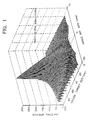
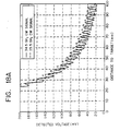
- the disclosed millimeter wave proximity sensor of the present invention provides at least a 6 times increase in detection range, relative to an inductive sensor, and its sensing range increases with target size, as optimally & theoretically shown by the graph in Fig. 1.
- the millimeter wave proximity sensor can detect a variety of materials, including metals, dielectrics and various liquids.
- Capacitive sensors have a greater range (1.6 inches max.) than an inductive sensor, as disclosed in The Basics of Inductive and Capacitive Proximity Presence Sensing , Eaton Corp. Milwaukee, Wisconsin, but are unsuitable for harsh environments due to the very significant and unacceptable effect that a harsh environment has on the operating mechanism of a capacitive sensor.
- Photoelectric and ultrasonic sensors rely on a non-absorbing and non-dispersive medium between their respective transmitter and the object to be detected. Most harsh environments are absorptive and dispersive, and hence are unsuitable for an ultrasonic or photoelectric proximity sensor.
- the harsh environments previously exemplified are essentially transparent to millimeter wave electromagnetic radiation and the millimeter wave proximity sensor of the present invention can function effectively in said environments to detect the presence or absence of an object.
- Doppler based microwave or millimeter wave sensors are intended for far field detection rather than near field (short range) detection of an object in motion and not for the detection of a stationary object.
- the Doppler type sensor is also not suitable for slow motion sensing due to detection sensitivity limitations incurred by the return signal being in a frequency region very close to the transmitter frequency.
- the signal frequency offset from the carrier decreases as the speed of the object in motion decreases.
- the sensor operational range is in what is known as the near field region of the transmitter output.
- the radiated wave is non-planar in the near field region. (It transitions to a plane wave in the far field.) Due to the non-uniform spatial field distribution, it is known that sensor detection nulls from an object will be experienced at some locations in the spatial range of the sensor.
- a unique feature of the disclosed proximity sensor is a means to alleviate these detection nulls.
- One of the objects of this invention is to provide a low power, low cost, millimeter wave (MMW) proximity sensor that provides over a 6:1 increase in minimum detection range (55 mm minimum) compared to standard 18 mm inductive proximity sensors.
- the design preferably includes a low cost MMW Gunn oscillator, MMW detector and analog processing/driver circuitry.
- the sensor is preferably designed for 3-wire operation and will fit in a standard 18 mm tube.
- the sensor provides approximately a 6:1 improvement in minimum detection range compared to 18 mm inductive sensors.
- a standard 18 mm inductive sensor would provide 9 mm of sensing range as compared to the MMW sensor which will provide 55 mm of sensing range.
- An important difference between the MMW proximity sensor and conventional inductive sensor technology is that the sensing range of the present invention is a function of target size. Therefore, the sensing range of the proximity sensor of the present invention will be significantly greater for larger targets (i.e. >30:1 theoretical improvement for a 100 mm target).
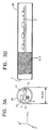
- FIG. 4 A perspective view of the low cost, low power, MMW Gunn oscillator of the present invention is presented in Figure 4.
- a simple monopole element is used as both the tuning circuit and interface between the Gunn diode and the output of the sensor. This greatly simplifies the circuit topology and therefore the assembly cost.
- This simple, robust circuit design results in a low manufactured cost and eliminates any need for circuit alignment
- Two breadboarded oscillators both achieved +10 dBm output power at 35 GHz, thus meeting a 0 dBm nominal output power design goal. Excellent repeatability was observed from breadboard to breadboard.
- FIG. 5 A perspective view of the low cost MMW detector circuit of the present invention is shown in Figure 5.
- the circuit was realized using a simple printed circuit and a low cost, commercially available, GaAs Schottky diode which was designed for pick and place type assembly. This resulted in an extremely simple, highly produceable, low cost circuit.
- Two breadboarded MMW detector circuits provided good sensitivity and very flat performance over the 30 to 37 GHz frequency range, thereby permitting a decrease in the oscillator frequency accuracy. Excellent repeatability was observed from breadboard to breadboard.
- the MMW proximity sensor and a photoelectric sensor product manufactured by Eaton Corporation are similar from a functional point of view. Due to this similarity, the Eaton photoelectric ASIC was able to be used in the analog processing/driver circuitry of the present invention. This greatly reduces the circuit complexity and therefore reduces the manufactured cost.
- a breadboard of the analog processor/driver circuits was built and evaluated. Initial results looked excellent and the board met all design goals.
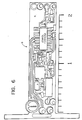
- a top plan view of the analog processor/driver board is presented in Figure 6.
- an electromagnetic wave, reflective type, active proximity sensor comprises:
- the two waveguide / two detector embodiment described above may be implemented in order to eliminate detection nulls.
- the particular embodiments of the receiver of the present invention, discussed herein, refer to a direct detection technique of detecting the reflected signal, it is to be understood that the receiver may be in the form of a homodyne mixer whereby the received signal is actually mixed with a delayed version of itself. Such a configuration may provide improved detector sensitivity.
- an electromagnetic wave, reflective type, active proximity sensor includes a transmitter, a receiver and means for substantially eliminating a leakage signal (i.e., portion of transmitted output signal that leaks into the receiver) which is received by the receiver after being radiated by the transmitter.
- a leakage signal i.e., portion of transmitted output signal that leaks into the receiver
- a beam splitter with a pre-determined thickness is positioned between the sensor and the target at a pre-determined separation distance. Accordingly, the output signal radiated by the transmitter strikes the beam splitter, and in response, the beam splitter generates a reflected signal portion and a transmitted signal portion. The transmitted signal portion continues on toward the target where it is reflected back to the sensor and received by the receiver.
- the reflected signal portion which is approximately 180 degrees out of phase with the leakage signal, reflects back to the receiver from the beam splitter and substantially cancels the leakage signal, resulting in improved detector sensitivity.
- the function of the beam splitter in one embodiment of the present invention, may be provided by the dielectric cover shown in Fig. 3b of the drawings.
- the transmitter and receiver each include a circular waveguide and a polarization circuit.
- the circular waveguide and polarization circuit of the transmitter serve to circularly polarize the output signal generated by the oscillator circuit in a first circular direction (i.e., either clockwise or counter-clockwise).
- the circularly polarized output signal is then radiated toward the target where it strikes the target and reflects back in the form of a return signal rotating in a second circular direction opposite to the first circular direction.
- the return signal is received by the circular waveguide of the receiver and circularly de-polarized (i.e., returned to a linear polarization) by the receiver polarization circuit.
- the circularly de-polarized signal is then processed by the detector. In this manner, the receiver is responsive only to signals polarized in the second circular direction and, thus, the leakage signal radiated by the transmitter, polarized in the first circular direction, is not de-polarized by the receiver and, therefore, not processed by the detector.
- an electromagnetic, reflective type, active proximity sensor includes a transmitter having a voltage controlled oscillator circuit which generates an output signal which is modulated such that the frequency of the output signal varies over time between a range of frequencies.
- a voltage controlled oscillator circuit which generates an output signal which is modulated such that the frequency of the output signal varies over time between a range of frequencies.
- return signals which correspond to the radiated energy reflected from the target and respectively exhibit one of the frequencies corresponding to the range of frequencies associated with the frequency varying, output signal radiated by the transmitter, are received by the receiver.
- the detector of the receiver averages the return signals and, in response, generates an output signal corresponding to the return signals.
- the output signal generated by the voltage controlled oscillator circuit may discretely vary between at least two frequencies or, in another embodiment, sinusoidally vary between at least two frequencies.
- another object of the present invention is to provide an oscillator circuit which oscillates, thereby generating an output signal, without the need for a separate resonator.
- the present invention provides a self-resonating oscillator circuit in the form of a novel Gunn oscillator circuit.
- the discrete circuit elements which will be described in greater detail later, preferably include a Gunn diode and a chip capacitor coupled by an inductive line having a length of approximately one quarter wavelength. It is to be appreciated that, in a preferred embodiment, the chip capacitor and the inductive line constitute a low pass filter for applying bias voltage to the Gunn diode.
- a post is coupled to the Gunn diode in order to provide the output signal, generated by the circuit, to a waveguide to which the circuit may be coupled.
- the oscillator circuit may be modified such that the Gunn diode may be replaced with other active elements such as an Impatt diode, an FET or an HEMT device, while still achieving the advantages of the present invention discussed herein.
- Figure 1 is a graph in three dimensions of the maximum range vs. target size and angle off axis for a conventional proximity sensor.
- FIG. 2 is a block diagram of the millimeter wave proximity sensor formed in accordance with one form of the present invention.
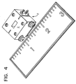
- Figure 3a is an assembly drawing, including an end view, of the millimeter wave proximity sensor of the present invention.
- Figure 3b is an assembly drawing, including a side view, of the millimeter wave proximity sensor of the present invention.
- Figure 4 is a perspective view of a first subassembly, namely, the Gunn oscillator, of the millimeter wave proximity sensor of the present invention.
- Figure 5 is a perspective view of a second subassembly, namely, the detector, of the millimeter wave proximity sensor of the present invention.
- Figure 6 is a top plan view of a third subassembly, namely, the analog processor/driver, of the millimeter wave proximity sensor of the present invention.
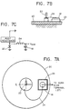
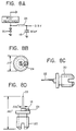
- Figure 7a is a top view of the Gunn oscillator circuit of the millimeter proximity sensor of the present invention.
- Figure 7b is a side view of the Gunn oscillator circuit of the millimeter wave proximity sensor of the present invention.
- Figure 7c is an equivalent schematic of the Gunn oscillator circuit of the millimeter wave proximity sensor of the present invention.
- Figure 8a is an equivalent schematic of the Gunn oscillator circuit of the millimeter wave proximity sensor of the present invention.
- Figure 8b is a top view of the Gunn oscillator circuit of the millimeter wave proximity sensor of the present invention.
- Figure 8c is a side view of the Gunn oscillator circuit of the millimeter wave proximity sensor of the present invention.
- Figure 8d is another side view of the Gunn oscillator circuit of the millimeter wave proximity sensor of the present invention.
- Figure 9a is an isometric assembly drawing of the Gunn oscillator circuit of the millimeter wave proximity sensor of the present invention.
- Figure 9b is a cross-sectional view of the Gunn oscillator circuit of the millimeter wave proximity sensor of the present invention.
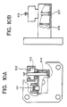
- Figure 10a is a front view, partially broken away, of a conventional Gunn oscillator circuit
- Figure 10b is a side view, partially broken away, of a conventional Gunn oscillator circuit.
- Figure 11 is a block diagram of another form of the proximity sensor of the present invention.
- Figure 12a is an end view of the form of the proximity sensor shown in Fig. 11.
- Figure 12b is a side view of the form of the proximity sensor shown in Fig. 11.
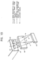
- Figure 13 is a perspective view of the proximity sensor of the present invention shown in Figures 11, 12a and 12b.
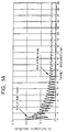
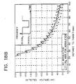
- Figure 14 is a graph of the detector output (volts) versus target distance (centimeters) for a proximity sensor formed in accordance with the present invention.
- Figure 15 is a block diagram of yet another form of the proximity sensor of the present invention.
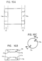
- Figure 16a is a side view of one embodiment of the dielectric card utilized in the polarization circuit of the present invention.
- Figure 16b is a cross sectional side view of another embodiment of the polarization circuit of the present invention.
- Figure 16c is a front view of the same embodiment of the polarization circuit illustrated in Figure 16b.
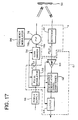
- Figure 17 is a block diagram of still a further form of the proximity sensor of the present invention.
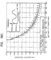
- Figures 18 a, b and c are graphs of the detected voltage (millivolts) versus the distance to the target (millimeters) for respective embodiments of the present invention.
- Figure 19 is a front view of yet another form of the proximity sensor of the present invention, combining the novel features of the proximity sensors respectively depicted in Figs. 15 and 17.
- Figure 20 is a front view of still a further form of the proximity sensor of the present invention.
- FIGs. 2, 3a and 3b A block diagram and assembly drawing of the millimeter wave proximity sensor of one form of the present invention are shown in Figs. 2, 3a and 3b. Views of the three sub-assemblies constituting the sensor, namely, the Gunn oscillator 2, detector circuit 4 and analog processor/driver 6 are shown in Figs. 4-6. Details of the Gunn oscillator circuit 2 are shown in Figs. 7a through 7c and 8a through 8d, and an assembly drawing of the Gunn oscillator 2 is shown in Fig. 9a and Fig. 9b.
- an electromagnetic wave, reflective type, active proximity sensor includes a transmitter for transmitting radiated energy to a target 50, the transmitter including a Gunn oscillator circuit 2, the Gunn oscillator circuit including a Gunn oscillator 52 and a Gunn driver 54 coupled to the Gunn oscillator 52.
- the Gunn oscillator 52 driven by the Gunn driver 54, generates a pulse modulated signal which is radiated by the transmitter to the target 50.
- the electromagnetic wave proximity sensor also includes a receiver, the receiver including first and second waveguides 12,14, and first and second detectors 8,10 respectively coupled to the first and second waveguides 12,14.
- the first and second waveguides 12,14 receive radiated energy reflected from the target 50 and provide the radiated energy to the first and second detectors 8,10, respectively.
- Each of the first and second detectors 8,10 generates an output signal which corresponds to the radiated energy received by the first and second waveguides 12,14.
- the receiver further includes a summer 56, the summer being coupled to the first and second detectors 8,10 and being responsive to the output signals of the first and second detectors.
- the summer 56 generates an output signal corresponding to the sum of the output signals of the first and second detectors 8,10.
- the electromagnetic wave proximity sensor also includes an analog processor/driver circuit 6.
- the analog processor/driver circuit is responsive to the output signal of the summer 56.
- the processor/driver circuit 6 includes a pulse modulator 58 generating a pulsed signal and providing the pulsed signal to the Gunn driver 54, an amplifier 60 receiving the output signal of the summer 56 and generating an amplified signal in response thereto, a synchronized demodulator signal conditioner 62 being responsive to the amplified signal and generating an output signal in response thereto, and an output stage 64 responsive to the output signal from the synchronized demodulator signal conditioner 62 and generating an output signal in response thereto.
- the output stage 64 provides a TTL pulsed output signal or in another logic compatible format to interface properly with external circuitry.
- the output stage may be Eaton Corporation Part No. 109905 and the rest of processor 6 may be Eaton Corporation Part No. 109744.
- a power supply 66 may be included to power the various components of the sensor.
- the sensor is preferably designed to operate at the millimeter wave frequency of 35 GHz.
- a Gunn diode is used as the active element in a pulsed oscillator that is used as a transmitter.
- the pulsed 35 GHz signal is radiated into the target area that is designed to extend from the face of the transmitter to a distance of approximately 12 inches.
- the transmitted signal is reflected back to the two detectors 8,10 contained in the two receive waveguides 12,14 in the sensor housing 16, as shown in Fig. 3a and Fig. 3b.
- a dielectric cover 7 is mounted on the sensor housing 16 at the face of the sensor.
- the target area of the sensor is in the near field region of the transmitter. It is known that in this close-in region there is a non-uniform spatial distribution of electromagnetic field as transmitter output transitions from the output waveguide port 18 of the transmitter to free space. It is also known that sensor detection nulls may result from the non-uniform spatial field distribution for an object in some locations of the sensing range.
- a unique feature ofthe sensor is the use of two detectors 8,10 in a two dimensional receive array (Fig. 3a) to alleviate the detection nulls in the near field region. The output of the detectors are series connected and summed.
- Fig. 3a includes a Cartesian graph illustrating the orientation of the X, Y and Z coordinates with respect to the sensor face. Particularly, the X axis is horizontal with respect to the sensor face, the Y axis is vertical with respect to the sensor face, and the Z axis is coaxial with respect to the length of the sensor housing. It is to be appreciated that other such configurations may achieve substantial elimination of null conditions.
- the two receive waveguides 12,14 may be respectively positioned to have only different X coordinates or different Y coordinates. Likewise, positioning the transmitter such that it has a different Z coordinate than the two receive waveguides 12,14 also may provide substantial elimination of null conditions. Still further, another embodiment of the present invention whereby the two receive waveguides 12,14 are positioned to have different Z coordinates, which are preferably approximately one quarter wavelength apart from each other, may also provide advantageous null condition elimination.
- Alternate means to eliminate any detection nulls in the spatial range of the sensor are to use a FSK (frequency shift keying) or broadband noise modulated transmitter source rather than the fixed frequency Gunn diode source as previously described.
- FSK modulation the RF frequency of the transmitter is shifted rapidly between one of two frequencies.
- a broadband noise modulated transmitter source would also provide an output with varying frequency content and would eliminate a detection null in the spatial range of the sensor in the manner described for FSK modulation.
- FSK or broadband noise modulation it would be possible to use one receiver rather than the two receiver configuration as previously described for a fixed frequency Gunn oscillator. A particular implementation of the FSK modulation technique will be described later, in greater detail, in the context of the embodiment of the present invention depicted in Fig. 17.
- Another means to eliminate detection nulls in the spatial range of the sensor is to chirp the output of the pulsed Gunn oscillator 2 over the width of the output RF pulse.
- pulsing of the RF output of the Gunn diode is accomplished by pulsing the bias voltage applied to the Gunn diode.
- a train of rectangular bias voltage pulses drives the Gunn diode bias from zero to a constant value of operating voltage during the width of the pulse.
- the RF frequency is constant over the duration of the pulse since bias voltage is constant.
- pulsed bias voltage that is not constant in amplitude is preferably used (e.g. trapezoidal pulse).
- Chirping of output frequency results from the known pushing characteristic of a Gunn oscillator (and other oscillator types) and is manifest by a change in oscillator frequency with the magnitude of the applied bias voltage.
- the sensor receiver would not experience a detection null since if a detection null occurs at a particular frequency, a null would not be present over the range of the other frequencies constituting the frequency chirp.
- this chirp technique it would be possible to use one receiver for the proximity sensor rather than the two receiver configuration previously described.
- RF leakage from the transmitter output waveguide port 18 directly into the receiver waveguide ports 12,14 is minimized by optimizing the longitudinal position of the transmitter port relative to the receiver ports. Minimizing the RF leakage will maximize the tangential sensitivity of the receiver.
- the 35 GHz transmitter source used in the sensor uses a Gunn diode as the active element in a novel oscillator circuit.
- the novel features of the Gunn diode oscillator 2 were previously delineated and a detailed description of the oscillator circuit is to follow.
- FIGs. 7a through 7c and 8a through 8d A circuit diagram and circuit layout of the oscillator 2 are presented in Figs. 7a through 7c and 8a through 8d.
- a perspective view of the assembled oscillator is shown in Fig. 4 and an assembly drawing is shown in Fig. 9a and Fig. 9b.
- the elemental form of the oscillator is evident from the small size of the oscillator circuit and the low parts count.
- the discrete circuit elements are a standard packaged Gunn diode 20 and a chip capacitor 18. As illustrated in Fig. 7a and Fig. 7b, the chip capacitor 18 is mounted on the Gunn diode 20 with a copper spacer 23 positioned therebetween.
- a thin and narrow metal post 22 e.g.
- the post 22 is sized such that its reactance in combination with Gunn diode and circuit reactances present a resonant circuit to the negative resistance of the Gunn diode 20 at the 35 GHz frequency of oscillation. It is preferred if the post 22 does not contact the top wall of the waveguide embodiment. Post length is a primary determinant of oscillator frequency. The shorter the length of the post, the higher is the oscillation frequency.
- Fig. 9a also illustrates the location and connectivity of the Gunn bias terminal 27 to the oscillator circuit via microcoax 31. Also shown in Fig. 9a is the location of the ground terminal 29 of the oscillator circuit.
- This arrangement is novel and different from that used in conventional Gunn oscillators, such as disclosed in Gunn Diode Circuit Handbook , No. HB-9000, Microwave Associates, where bias is applied to the Gunn diode via a metal post that contacts the top cap of the Gunn diode and extends through and is insulated from the top wall of the waveguide.
- the portion of the post extending outward from the top wall is fabricated as a coaxial line with low and high impedance quarter wave sections that constitute a low pass filter for applying basis to the Gunn diode.
- This conventional biasing arrangement is illustrated in Fig. 10a and Fig. 10b and is from the Gunn Diode Circuit Handbook referenced above.
- the conventional biasing arrangement as illustrated in Figs. 10a and 10b, includes a tuner 101, a bypass 102, a choke 103, a post coupling 104, a bias terminal 105, an iris hole 106 and a diode 107.
- This biasing arrangement is more complex and expensive to fabricate and assemble than the chip capacitor arrangement, disclosed herein, and therefore is unsuitable for an oscillator where low cost is a primary objective.
- the non-contacting nature of the post 22 to the top wall of the waveguide in the present invention provides a simple means by which the oscillator can be provided with self-compensation of the frequency change that is known to occur with oscillators due to changes in temperature. Frequency compensation with temperature change is accomplished in the following manner.
- the post 22 in the present invention was of the same material as the waveguide embodiment (e.g. copper), the gap between the top wall of the waveguide and the top of the post would increase with temperature due to the difference in length between the height of the waveguide and the height of the post.
- An increase in gap size has been measured to result in an increase in oscillator frequency.
- Simultaneous with this thermal expansion is the expansion of the waveguide length between the post and the fixed back short 25 (Fig. 9b) which causes a decrease in oscillator frequency.
- the coefficient of thermal expansion is 16.8 x 10 -6 /°C and for a post made of Invar the coefficient is 0.9 x 10 -6 /°C.
- the gap between the top wall of the waveguide and the post will be larger with a temperature increase than that with a copper post.
- the larger gap will produce a larger increase in oscillator frequency relative to that with a copper post and will offset the decrease in frequency that is characteristic of the uncompensated oscillator. Frequency/temperature compensation in this new oscillator circuit is accomplished without the addition of any additional parts to the uncompensated oscillator.
- the measured external Q factor of the oscillator 2 was 110.
- the measured output power of several oscillators indicates that the oscillators are critically coupled (matched) to the output waveguide load.
- Conventional Gunn oscillators use an appropriately spaced coupling iris at the output port of the oscillator to match the oscillator to the output load, as shown in Fig. 10b.
- the oscillator of the present invention described herein does not require a coupling iris or any other matching network to establish a matched condition.
- the matched condition required for maximum output power is indicated to be inherent to the oscillator circuit.
- the Gunn diodes used in these oscillators were tested by the vendor in their standard critically coupled (matched) cavity oscillator. The output power measured by the vendor under these conditions was near equal to the output power measured in the oscillator circuit disclosed herein.
- the oscillator 2 could be operated without any external isolation between the load and the oscillator (e.g. ferrite isolator) into high VSWR loads (at least 4.5:1) without significant disturbance of oscillator performance.
- the pulling of the oscillator was ⁇ 30 MHZ, corresponding to 0.094% of oscillation frequency (35 GHz).
- Pulling of an oscillator is the change in oscillator frequency that results when a load of a given VSWR is changed through all phase ( ⁇ 180 degrees).
- the good pulling characteristics of the oscillator is indicated as also being intrinsic to the oscillator circuit.
- the millimeter wave proximity sensor design of the present invention described previously has been modified in a further embodiment of the present invention for the purpose of increasing its detection sensitivity and simplifying its form which decreases its cost and size.
- the new upgraded configuration contains only one waveguide receiver 30 and one millimeter wave detector 32.
- Block diagrams and layouts of this alternative embodiment of the proximity sensor and that which was previously disclosed are shown in Figs. 11, 12a and 12b and Figs. 2, 3a and 3b, respectively.
- the design shown in Figs. 11, 12a and 12b, the one receiver configuration is the preferred form for the proximity sensor.
- a larger waveguide (WR-28) 34 is used for the transmitter than is used for the receiver (WR-22) 30 for the 35 GHz prototype sensor in order to narrow the transmitter beamwidth and thereby obtain a larger target return and minimize false target returns.
- the new configuration (Figs. 11, 12a and 12b) is simpler, lower cost and exhibits higher detection sensitivity than the previously disclosed design (Figs. 2, 3a and 3b).
- the increase in detection sensitivity follows from the use of a unique means to decrease to an insignificant level the transmitter signal that leaks directly into the receiver waveguide port 30. Said leakage is significantly less than that experienced with the previous design using two receivers 12,14 (Figs. 2, 3a and 3b).
- the leakage of transmitter signal into the receiver port(s) deteriorates sensor performance since it limits the minimum level of target return that can be detected.
- transmitter to receiver leakage contributes to the amplitude of the ripple that is present in normal sensor operation as a function of sensor to target distance. Since ripple amplitude limits the performance capability of the sensor (e.g. range setability, hysteresis), it is preferred that transmitter to receiver leakage be reduced to an insignificant level.
- a dielectric beam splitter 36 is spaced approximately a quarter wavelength from the transmitter and receiver waveguide ports 34,30 in the face 38 of the sensor housing.
- a direct leakage path from the transmitter to the receiver port is shown by dashed line D, said leakage resulting in a degradation of sensor performance.
- the main beam from the transmitter (solid line A) impinges upon the beam splitter 36 which is a low loss dielectric plate (e.g. Lexan). Most of the transmitter signal passes through the plate to the target 40.
- the target return to the receiver port is shown by solid line B. A small portion of the main beam is reflected back to the receiver port 30 (dashed line C).
- the plate thickness is approximately half wavelength in the dielectric and is sized to provide the desired level of reflected signal. With the dielectric plate 36 spaced near a quarter wavelength from the receiver port 30, the reflected energy is 180° out of phase with the direct leakage signal and hence, nullifies the effect of the transmitter leakage on sensor performance. The effective isolation between transmitter and receiver ports 34,30 has been measured to be more than 40 dB with this means of leakage suppression. It should be appreciated that the dielectric cover 7 (Fig. 3b) may function as the beam splitter 36 in an alternative embodiment of the present invention.
- the design of the proximity sensor was described at 35 GHz, the design can be implemented at any millimeter wave, submillimeter wave or microwave frequency.
- the design described used a Gunn diode as the active element, other active elements such as Impatt diode, FET or HEMT devices can also be used.
- Figs. 15 and 17 are block diagrams depicting two alternative forms of the proximity sensor of the present invention providing such increased isolation
- Fig. 19 is a front view of another form of the proximity sensor of the present invention which combines the novel features of the sensors respectively depicted in Figs. 15 and 17.
- Fig. 14 is a graph illustrating the detector output of the sensor (i.e., detected voltage) as a function of target distance from the sensor. Specifically, two curves are shown, one curve illustrates the detector output of a sensor having 30 dB of isolation, while the other curve illustrates the same for a sensor having 45 dB of isolation. As is evident from the graph, the sensor having a higher isolation exhibits less ripple with respect to the detector output than that of the sensor with lower isolation and is, therefore, less likely to experience ripple-causing detection problems. It is to be appreciated that the embodiments of the proximity sensor illustrated in Figs. 15, 17 and 19 implement techniques which serve to substantially minimize the effect of the above-described ripple by increasing the transmit to receive isolation of the sensor.
- the proximity sensor depicted therein implements a novel cross-polarization technique which achieves a substantial improvement in the isolation between the transmitter and the receiver. It is to be appreciated that such isolation improvement increases the detection sensitivity of the proximity sensor. It should also be noted that components illustrated in Fig. 15 having the same reference designation numbers as components illustrated in previously discussed embodiments are functionally the same components.
- the electromagnetic wave, reflective type, active proximity sensor of Fig. 15 includes a transmitter for transmitting radiated energy to a target 50.
- the transmitter includes a Gunn oscillator circuit 2 and a transmitter polarization circuit 70 coupled to the Gunn oscillator circuit 2. The structure of the transmitter polarization circuit will be described in greater detail later.
- the Gunn oscillator circuit 2 is structurally and functionally the same as the Gunn oscillator circuit described with respect to both Fig. 2 and Fig. 11.
- the Gunn oscillator circuit 2 itself, includes a Gunn oscillator 52 and a Gunn driver 54 coupled to the Gunn oscillator 52.
- the transmitter also includes a circular waveguide 80 (Fig. 19) coupled to the Gunn oscillator circuit 2, in which the transmitter polarization circuit 70 is preferably located and from which the radiated energy is transmitted.
- the electromagnetic wave proximity sensor illustrated in Fig. 15 also includes a receiver, the receiver including a receiver polarization circuit 72 and a detector 32 coupled to the receiver polarization circuit 72.
- the structure of the receiver polarization circuit will be described in greater detail later.
- the receiver also includes a circular waveguide 82 (Fig. 19) coupled to the detector 32, in which the receiver polarization circuit 72 is preferably located and by which the radiated energy reflected from the target 50 is received.
- the proximity sensor of Fig. 15 includes an analog processor/driver circuit 6.
- the analog processor/driver circuit 6 is structurally and functionally the same circuit as was previously described with respect to the proximity sensor embodiments depicted in Figs. 2 and 11.
- the analog processor/driver circuit 6 includes an amplifier 60 coupled to the detector 32 of the receiver, a synchronous demodulator signal conditioner 62 coupled to the amplifier 60, and an output stage 64 coupled to the synchronous demodulator signal conditioner 62.
- the analog processor/driver circuit 6 also includes a pulse modulator 58 coupled to both the synchronous demodulator signal conditioner 62 and the Gunn driver 54 of the transmitter.
- Power supply 66 is connected to the various components of the sensor and provides the necessary input power to each of the above-described components which require the same.
- the electromagnetic wave proximity sensor illustrated in Fig. 15 operates in the following manner.
- the pulse modulator 58 generates a pulsed signal and provides the pulsed signal to the Gunn driver 54.
- the Gunn oscillator 52 in response to being driven by the Gunn driver 54, generates a pulse modulated signal.
- the circular waveguide 80 coupled to the Gunn oscillator circuit 2, propagates the pulse modulated signal to the transmitter polarization circuit 70 preferably located in the circular waveguide 80.
- the pulse modulated signal generated by the Gunn oscillator circuit 2 is a linearly polarized signal.
- the transmitter polarization circuit 70 circularly polarizes the pulse modulated signal such that the signal rotates in a first circular direction.
- the first circular direction may be either a clockwise or a counter-clockwise rotation.
- the circularly polarized, pulse modulated signal is then radiated from the circular waveguide 80 toward the target 50, whereby the signal strikes the target 50 and reflects back toward the proximity sensor.
- the signal changes its rotational sense and rotates in a second circular direction.
- the second circular direction is opposite to the rotational sense of the first circular direction and, thus, may be either a clockwise or counter-clockwise rotation.
- the circular waveguide 82 of the receiver receives the radiated energy reflected from the target 50 in the form of the circularly polarized, pulse modulated signal rotating in the second circular direction.
- the receiver polarization circuit 72 is located in the circular waveguide 82 and its preferred structure will be described later in greater detail.
- the receiver polarization circuit 72 is responsive to the circularly polarized, pulse modulated signal rotating in a second circular direction and removes the circular polarization associated therewith. It is to be appreciated that the receiver of the embodiment illustrated in Fig. 15 is responsive only to signals which are polarized in the same rotational sense as the receiver polarization circuit 72 (i.e., in the second circular direction).
- the return signal after being circularly de-polarized, is passed from the receiver polarization circuit 72 to the detector 32 by the circular waveguide 82.
- the detector 32 generates an output signal which corresponds to the radiated energy reflected back from the target 50 in the form of the circularly polarized, pulse modulated signal rotating in a second circular direction (i.e., the return signal).
- the analog processor/driver circuit 6 is responsive to the output signal generated by the detector 32. Specifically, the amplifier 60 of the analog processor/driver circuit 6 receives the output signal of the detector 32 and generates an amplified signal in response thereto. Next, the synchronous demodulator signal conditioner 62 receives the amplified signal and, in response thereto, generates its own output signal. The output signal generated by the synchronous demodulator signal conditioner 62 is then received by the output stage 64 and, in response thereto, the output stage 64 generates an output signal. As previously discussed with respect to the above-described embodiments of the present invention, the output stage 64 preferably provides a TTL pulsed output signal (or some other logic compatible format) such that the proximity sensor may be properly interfaced with external circuitry. Also, as previously mentioned, Eaton Corporation Part No. 109905 may be used as the output stage 64 illustrated in Fig. 15, while the rest of the analog processor/driver 6 may be Eaton Corporation Part No. 109744.
- the transmitter polarization circuit 70 preferably includes a thin dielectric card (injection molded Nylon 6/6) of a predetermined length which is inserted into the circular waveguide 80 at a 45 degree angle relative to the dominant mode electric field of the signal generated by the Gunn oscillator circuit 2.
- Fig. 16a is a side view of a preferred embodiment of the dielectric card, which will be described in greater detail later.
- the electric field associated with the pulse modulated signal generated by the Gunn oscillator circuit 2, which is present in the circular waveguide 80 can be decomposed into two orthogonal components, one which is perpendicular to the dielectric card and the other which is parallel to the dielectric card.
- the entire electric field will rotate in a circular manner. Accordingly, in this manner, the signal is circularly polarized. It should also be appreciated that if the dielectric card is placed in the circular waveguide 80 at the opposite 45 degree angle relative to the electric field, the entire electric field will rotate in the opposite direction and, therefore, have an opposite circular polarization as compared to that of the field circularly polarized by the dielectric card inserted in the initially-described position.
- the dielectric card illustrated in Fig. 16a preferably includes a first matching section 74 and a second matching section 76, whose functions will now be described.
- the matching sections, 74 and 76, illustrated in Fig. 16a are included in order to respectively reduce signal reflection due to the difference between the dielectric constant associated with the material used to produce the dielectric card and the dielectric constant associated with free space.
- the first matching section 74 provides an intermediate dielectric constant which presents more of a gradual transition, between free space and the dielectric material, for the pulse modulated signal propagating through the circular waveguide 80.
- the intermediate dielectric constant is provided by notching the dielectric card in the manner illustrated in Fig. 16a, thus producing cutout 74a.
- the second matching section 76 includes cutout 76a which similarly provides for a more gradual transition for the propagating signal.
- the receiver polarization circuit 72 includes the same dielectric card as described with respect to the transmitter polarization circuit 70 and as illustrated in Fig. 16a.
- the dielectric card of the receiver polarization circuit 72 is inserted into the circular waveguide 82 at a 45 degree angle which is opposite (90 degrees offset) to the 45 degree angle of the dielectric card inserted in the circular waveguide 80 of the transmitter.
- the circular waveguides of the transmitter and the receiver, 80 and 82 are oppositely polarized and are, therefore, said to be cross-polarized.
- the dielectric card inserted in the receiver waveguide 82 utilizes the first and second matching sections, 74 and 76, to reduce reflection and provide a gradual transition for the signal passing therethrough.
- the present invention encompasses alternative forms of the transmitter and receiver polarization circuit 70 and 72.
- the dielectric card described above may be integrally formed with a dielectric cover (i.e., single piece), similar to the dielectric cover 7 (Fig. 3b), which respectively fits over the openings of the circular waveguides.
- the polarization circuit may be implemented as illustrated in Figs. 16b and 16c. Figs. 16b and 16c respectively illustrate a cross sectional side view and a front view of another embodiment of the polarization circuit whereby dielectric fins 75a and 75b are preferably integrally formed on the inner surface of the circular waveguides.
- Fig 16b is a cross sectional side view taken along the line 16b-16b shown in Fig 16c.
- the dielectric fins, 75a and 75b are positioned at a 45 degree angle relative to the dominant mode electric field as described above with respect to the dielectric card. It is to be appreciated that Figs. 16b and 16c illustrate only one of the circular waveguides and that the other circular waveguide will have similarly formed dielectric fins that are positioned 90 degrees offset from the first waveguide in a similar manner as described with respect to the dielectric cards.
- the dielectric fins 75a and 75b extend into the waveguide approximately less than one third of the inner diameter of the waveguide.
- these dielectric fins also referred to as one quarter wavelength plates, have cutouts 77a, b, c and d, similar to the cutouts, 74a and 76a, illustrated in Fig. 16a. Cutouts 77a - d provide a similar matching function as described above.
- the circular polarization of a signal passing through a polarization circuit as depicted in Figs. 16b and 16c is accomplished in the same way as described above with respect to the dielectric card.
- the above described embodiments of the polarization circuit of the present invention may also be implemented in a square waveguide, rather than a circular waveguide.
- the isolation of the proximity sensor is increased by approximately 20 dB to 25 dB, thus resulting in a minimum isolation of approximately 45 dB (i.e., without the need for any special or critical alignment). Accordingly, such a proximity sensor formed in accordance with the present invention will be less likely to experience the ripple-causing detection problems previously discussed. Further, this cross-polarization technique is not frequency sensitive since the polarization circuits, 70 and 72, are operable over the entire operational frequency bandwidth of the proximity sensor contemplated by the present invention.
- FIG. 17 another alternative form of the present invention, employing a frequency modulation technique, is illustrated therein.
- the embodiment of the present invention illustrated in Fig. 17 is structurally the same as the embodiment illustrated in Figs. 11, 12a and 12b, with the exception of the transmitter.
- a Gunn voltage controlled oscillator (VCO) 78 is employed in place of the Gunn oscillator 52 (Fig. 11).
- the Gunn VCO 78 includes a bias port 78a and a tuning port 78b.
- the Gunn driver 54 is coupled to the bias port 78a of the Gunn VCO 78, while a frequency modulator 84 is coupled to the tuning port 78b of the Gunn VCO 78.
- the transmitter includes waveguide 34 (Fig. 12a) and the receiver includes waveguide 30 (Fig. 12a).
- the frequency modulation technique described in the context of the sensor depicted in Fig. 17 provides a significant improvement in isolation between the transmitter and the receiver.
- the concept behind this novel frequency modulation technique is that the phase of the return signal (i.e., signal reflected from the target) relative to the leakage signal can be changed, at a specific distance from the sensor, without physically moving the target or sensor. This is accomplished in the present invention by shifting the frequency of the oscillator of the transmitter in a particular manner that will be described later. For instance, if at some distance R from the sensor the return signal is 180 degrees out of phase with the leakage signal, then the detected voltage will be at a minima.
- the phase of the return signal obeys an e -2jkr dependence, where j equals ⁇ -1, k equals the freespace wave propagation constant in mm -1 and r equals the distance from the transmitter to the target in mm, it can be seen from this relationship that the phase cycles at a rate of 2r, due to the round trip path (i.e., from the sensor to the target and back to the sensor) and, therefore, one quarter wavelength of distance results in a 180 degree shift in phase.
- the frequency deviation required to shift the return signal phase by 180 degrees corresponds to the frequency at which the target distance is equal to one quarter wavelength.
- c equal to the speed of light in air (3 x 10 11 mm/sec)
- R is the distance between the sensor and the target in millimeters (mm).
- a 1GHz shift in frequency will result in a 180 degree phase shift in the return signal.
- Fig. 18a is a graph representing the respective theoretical responses of a proximity sensor of the present invention at two frequencies, 34.5 GHz and 35.5 GHz, that are separated by 1GHz. As is evident from the graph, the two signals are 180 degrees out of phase with each other at 75 mm.
- the Gunn driver 54 coupled to the bias port 78a of the Gunn VCO 78, generates a signal which biases (i.e., turns on and off) the Gunn VCO 78.
- the frequency modulator 84 coupled to the tuning port 78b of the Gunn VCO 78, provides a modulating signal to the Gunn VCO 78.
- the Gunn VCO 78 generates an output signal in response to the Gunn driver 54 and the frequency modulator 84.
- the frequency of the output signal generated by the Gunn VCO 78 is proportional to the value of the voltage applied to the tuning port 78b.
- the output signal of the Gunn VCO 78 will be a function of the modulating signal provided by the frequency modulator 84 and, thus, a frequency varying output sigma.
- the Gunn VCO 78 in a preferred embodiment, is a lumped element VCO and is varactor-tuned over a frequency range of 32 GHz to 38 GHz, providing a nominal output power of +5 dBm.
- the detector 32 can only respond to the average of the two detected waveforms, i.e., one detected waveform being attributed to a return signal reflected from the target exhibiting the first discrete frequency and the other detected waveform being attributed to a return signal reflected from the target exhibiting the second discrete frequency. Therefore, over a small range encompassing the distance where the two return signals are 180 degrees out of phase with each other, the output signal generated by the detector 32 will exhibit substantially no ripple.
- FSK modulation of the Gunn VCO output signal can be accomplished by applying a square wave signal, generated by the frequency modulator 84, to the tuning port 78b of the Gunn VCO 78.
- Fig. 18b is a graph representing the theoretical response of a proximity sensor of the present invention whose transmitted signal is FSK modulated over a frequency deviation of 1GHz (34.5 GHz and 35.5 GHz). A curve illustrating a response without FSK modulation is also included for comparison.
- the detector 32 does in fact respond to the average value of the two return signals as evidenced by the substantially flat (i.e., substantially ripple free) region around 75 mm.
- the substantially flat region will repeat itself at each distance interval that corresponds to an odd multiple of quarter wavelengths of the deviation frequency.
- the distance where substantially no ripple occurs can be precisely controlled, in accordance with the present invention, by selecting the appropriate frequency deviation.
- the analog processor/driver circuit 6 is responsive to the output signal generated by the detector 32, whereby the amplifier 60 receives the output signal of the detector 32 and generates an amplified signal in response thereto.
- the synchronous demodulator signal conditioner 62 receives the amplified signal and, in response thereto, generates an output signal.
- the output signal generated by the synchronous demodulator signal conditioner 62 is then received by the output stage 64 and, in response thereto, the output stage 64 generates an output signal in a format compatible with external circuitry.
- Eaton Corporation Part No. 109905 may be used as the output stage 64 illustrated in Fig. 17, while the rest of the analog processor/driver 6 may be Eaton Corporation Part No. 109744.
- the detector 32 will average the detected waveforms over the entire range of the frequency output spectrum. It should be understood that the weighting at each frequency will be proportional to the shape of the modulation waveform and is determined by how much of the transmitted pulse is occupied by a particular frequency deviation. This results in the averaging of a continuum of phase shifts at each distance and, thus, can provide lower ripple over broader regions of the sensing distance. For example, Fig.
- 18c is a graph representing the theoretical response of a proximity sensor of the present invention whose transmitted signal is sinusoidally modulated over a deviation frequency bandwidth of 3 GHz (i.e., from 32 GHz to 35 GHz).
- a curve illustrating a response without any modulation (i.e., continuous wave (CW) operation at 35 GHz) is also included for comparison.
- the ripple is significantly reduced over an appreciable portion of the proximity sensor's preferred sensing distance of 0 to 80 mm.
- this novel frequency modulation technique serves to significantly reduce the ripple over a predictable, controllable and appreciable portion of the sensing range of the proximity sensor, thereby resulting in an effective increase of the sensor transmit-to-receive isolation by more than 15 dB. It is to be appreciated that other modulation shapes such as sawtooth or triangular waves may result in more optimum performance as compared to the sinusoidal modulation approach.
- FIG. 19 yet another embodiment of the electromagnetic wave proximity sensor, formed in accordance with the present invention, is illustrated. It is to be appreciated that this particular embodiment combines the cross-polarization technique employed in the proximity sensor illustrated in Fig. 15 and the frequency modulation technique employed in the proximity sensor illustrated in Fig. 17. Specifically, Fig. 19 is a front view (i.e., looking into the face of the sensor) of such a proximity sensor.
- the transmitter waveguide 34 employed in the sensor of Fig. 17 is replaced with the transmitter circular waveguide 80 (Fig. 15) which also includes the transmitter polarization circuit 70 (i.e., dielectric card illustrated in Fig. 16).
- the receiver waveguide 30 employed in the sensor of Fig. 17 is replaced with the receiver circular waveguide 82 (Fig. 15) which also includes the receiver polarization circuit 82 (i.e., dielectric card illustrated in Fig. 16).
- the output signal generated by the Gunn VCO 78 is both frequency modulated and circularly polarized in the novel manners previously described.
- the circular waveguide 80 in a preferred embodiment, is designed to pass only the second harmonic of the signal generated by the Gunn VCO 78, e.g., if the signal generated has a fundamental frequency range of 27 GHz to 32 GHz, then the transmitted signal will exhibit a second harmonic frequency range of 54 GHz to 64 GHz.
- Fig. 19 illustrates a transmitter E-plane (i.e., electric field) probe 90.
- the E-plane probe 90 transforms the mode of the signal generated by the Gunn VCO 78 (i.e., microstrip mode) to waveguide mode such that the signal may be propagated through the circular waveguide 80 to the polarization circuit 70.
- Fig. 19 also illustrates a receiver E-plane probe 92.
- the E-plane probe 92 transforms the return signals received by the circular waveguide 82 from waveguide mode to microstrip mode such that the detector 32 may process the return signals.
- Fig. 19 illustrates the E-plane probes, 90 and 92, 180 degrees offset from one another.
- the signal generated by the Gunn VCO 78 is a linearly polarized signal prior to being circularly polarized by the transmitter polarization circuit 70.
- the return signal becomes a linearly polarized signal after passing through the receiver polarization circuit 72.
- an additional 20 dB in isolation may be realized.
- the orthogonally disposed E-plane probes, 90 and 92 should preferably be approximately one quarter wavelength long in order to achieve the above-described additional isolation.
- the proximity sensor as depicted in Fig. 19 and Fig. 20, by employing the above-described cross-polarization and frequency modulation techniques in accordance with the present invention, may advantageously provide effective transmitter-to-receiver isolation in excess of 50 to 55 dB over the desired sensing range.
- the receiver of the present invention refers to a direct detection technique of detecting the reflected signal
- the receiver may be in the form of a homodyne mixer whereby the received signal is actually mixed with a delayed version of itself.
Abstract
Description
- This invention is directed to an electromagnetic wave proximity sensor. In the context of this invention, the term "electromagnetic wave" includes both "microwave" and "millimeter wave," as well as other frequencies. Further, in the context of this invention, the term "microwave" refers to a frequency of less than about 30 GHz, and "millimeter wave" refers to a frequency greater than about 30 GHz. In order to keep the size of the proximity sensor as small as possible, the invention preferably operates at frequencies above about 30 GHz (millimeter wave). Hence, the following description of the invention will refer to the proximity sensor as being a "millimeter wave" proximity sensor, in order to simplify the description, but it should be realized that the invention is not limited to frequencies above about 30 GHz, or millimeter waves, and proximity sensors including the features of this invention operating at different frequencies are envisioned to be within the scope of this invention.
- A proximity sensor is a non-contacting device for detecting the presence or absence of an object. Proximity sensors presently in use are of the following types:
- a) Capacitive
- b) Inductive
- c) Photoelectric
- d) Ultrasonic
- e) Microwave Doppler (Motion)
- It is the purpose of the new millimeter wave (frequency greater than 30 GHz) active proximity sensor, herein disclosed, to provide short range (from face of sensor to a few feet) sensing capability in a harsh environment, said capability not being presently available with known proximity sensors. The new features of the millimeter wave sensor are as follows:
- 1) A means for short range proximity sensing in harsh industrial or natural environments such as dust (e.g. grainery, mines), smoke, fog, vapor (e.g. degreaser, steam, hydrocarbon exhaust), hydrocarbon fluids (oil, grease), cleaning liquids or sprays (hydrocarbon or organic based, e.g. carbon tetrachloride, benzene, xylene, trichlorethylene), dirt, flames (fire fighting, furnaces).
- An inductive type proximity sensor may be used in a harsh environment but it lacks in sensor range (0.6 inches typical for a 30mm sensor diameter). The inductive sensor is also known to detect only metallic objects and that an increase in target size will not produce an increase in sensing range. The disclosed millimeter wave proximity sensor of the present invention provides at least a 6 times increase in detection range, relative to an inductive sensor, and its sensing range increases with target size, as optimally & theoretically shown by the graph in Fig. 1. In addition, the millimeter wave proximity sensor can detect a variety of materials, including metals, dielectrics and various liquids.
- Capacitive sensors have a greater range (1.6 inches max.) than an inductive sensor, as disclosed in The Basics of Inductive and Capacitive Proximity Presence Sensing, Eaton Corp. Milwaukee, Wisconsin, but are unsuitable for harsh environments due to the very significant and unacceptable effect that a harsh environment has on the operating mechanism of a capacitive sensor. Photoelectric and ultrasonic sensors rely on a non-absorbing and non-dispersive medium between their respective transmitter and the object to be detected. Most harsh environments are absorptive and dispersive, and hence are unsuitable for an ultrasonic or photoelectric proximity sensor. By contrast, the harsh environments previously exemplified are essentially transparent to millimeter wave electromagnetic radiation and the millimeter wave proximity sensor of the present invention can function effectively in said environments to detect the presence or absence of an object.
- Doppler based microwave or millimeter wave sensors are intended for far field detection rather than near field (short range) detection of an object in motion and not for the detection of a stationary object. The Doppler type sensor is also not suitable for slow motion sensing due to detection sensitivity limitations incurred by the return signal being in a frequency region very close to the transmitter frequency. The signal frequency offset from the carrier decreases as the speed of the object in motion decreases.
- 2) A means to provide uniform detected output of an object arbitrarily located in the spatial range of the millimeter wave proximity sensor herein disclosed.
- The sensor operational range is in what is known as the near field region of the transmitter output. There is a known spatial non-uniformity of the electromagnetic field in this near field region as the output of the transmitter transitions from the transmitter output waveguide port to free space. The radiated wave is non-planar in the near field region. (It transitions to a plane wave in the far field.) Due to the non-uniform spatial field distribution, it is known that sensor detection nulls from an object will be experienced at some locations in the spatial range of the sensor. A unique feature of the disclosed proximity sensor is a means to alleviate these detection nulls.
- 3) A means to provide a low cost transmitter source for the disclosed sensor. It is based on a new Gunn diode oscillator circuit with the following novel features:
- A means for self frequency compensation with temperature.
- Elimination of the need for an output isolator that is conventionally required to prevent excessive frequency change, frequency discontinuity or performance drop out with changes in output load.
- Elimination of the need for a matching circuit between the output waveguide and the oscillator circuit. A matching circuit is conventionally used to ensure maximum output power to the load.
- Use of the Gunn oscillator output waveguide directly as a slot type antenna, thereby eliminating the need for an external antenna
- Use of a Gunn oscillator waveguide circuit that has been reduced to an elemental form. The discrete circuit elements are a Gunn diode and a chip capacitor.
- One of the objects of this invention is to provide a low power, low cost, millimeter wave (MMW) proximity sensor that provides over a 6:1 increase in minimum detection range (55 mm minimum) compared to standard 18 mm inductive proximity sensors. The design preferably includes a low cost MMW Gunn oscillator, MMW detector and analog processing/driver circuitry. The sensor is preferably designed for 3-wire operation and will fit in a standard 18 mm tube.
- An initial cost analysis of the sensor assembly has been completed and results indicate that a manufactured cost of less than $100, in quantities of greater than 10,000, can be achieved.
- The sensor provides approximately a 6:1 improvement in minimum detection range compared to 18 mm inductive sensors. For an 18 mm target, a standard 18 mm inductive sensor would provide 9 mm of sensing range as compared to the MMW sensor which will provide 55 mm of sensing range. An important difference between the MMW proximity sensor and conventional inductive sensor technology is that the sensing range of the present invention is a function of target size. Therefore, the sensing range of the proximity sensor of the present invention will be significantly greater for larger targets (i.e. >30:1 theoretical improvement for a 100 mm target).
- A perspective view of the low cost, low power, MMW Gunn oscillator of the present invention is presented in Figure 4. A simple monopole element is used as both the tuning circuit and interface between the Gunn diode and the output of the sensor. This greatly simplifies the circuit topology and therefore the assembly cost. This simple, robust circuit design results in a low manufactured cost and eliminates any need for circuit alignment Two breadboarded oscillators both achieved +10 dBm output power at 35 GHz, thus meeting a 0 dBm nominal output power design goal. Excellent repeatability was observed from breadboard to breadboard.
- A perspective view of the low cost MMW detector circuit of the present invention is shown in Figure 5. The circuit was realized using a simple printed circuit and a low cost, commercially available, GaAs Schottky diode which was designed for pick and place type assembly. This resulted in an extremely simple, highly produceable, low cost circuit. Two breadboarded MMW detector circuits provided good sensitivity and very flat performance over the 30 to 37 GHz frequency range, thereby permitting a decrease in the oscillator frequency accuracy. Excellent repeatability was observed from breadboard to breadboard.
- The MMW proximity sensor and a photoelectric sensor product manufactured by Eaton Corporation are similar from a functional point of view. Due to this similarity, the Eaton photoelectric ASIC was able to be used in the analog processing/driver circuitry of the present invention. This greatly reduces the circuit complexity and therefore reduces the manufactured cost. A breadboard of the analog processor/driver circuits was built and evaluated. Initial results looked excellent and the board met all design goals. A top plan view of the analog processor/driver board is presented in Figure 6.
- In accordance with one form of the invention, an electromagnetic wave, reflective type, active proximity sensor comprises:
- a transmitter for transmitting radiated energy to a target, the transmitter including a Gunn oscillator circuit, the Gunn oscillator circuit including a Gunn oscillator and a Gunn driver coupled to the Gunn oscillator, the Gunn oscillator, driven by the Gunn driver, generating a pulse modulated signal which is radiated by the transmitter to the target;
- a receiver, the receiver including first and second waveguides and first and second detectors respectively coupled to the first and second waveguides, the first and second waveguides receiving radiated energy reflected from the target and providing the radiated energy to the first and second detectors, respectively, each of the first and second detectors generating an output signal which corresponds to the radiated energy received by the first and second waveguides, the receiver further including a summer, the summer being coupled to the first and second detectors and being responsive to the output signals of the first and second detectors, the summer generating an output signal corresponding to the sum of the output signals of the first and second detectors; and
- an analog processor/driver circuit, the analog processor/driver circuit being responsive to the output signal of the summer, the processor/driver circuit including a pulse modulator generating a pulsed signal and providing the pulsed signal to the Gunn driver, an amplifier receiving the output signal of the summer and generating an amplified signal in response thereto, a synchronized demodulator signal conditioner being responsive to the amplified signal and generating an output signal in response thereto, and an output stage responsive to the output signal from the synchronized demodulator signal conditioner and generating an output signal in response thereto.
- It is to be appreciated, as will be described in greater detail later, that the two waveguide / two detector embodiment described above may be implemented in order to eliminate detection nulls. Further, while the particular embodiments of the receiver of the present invention, discussed herein, refer to a direct detection technique of detecting the reflected signal, it is to be understood that the receiver may be in the form of a homodyne mixer whereby the received signal is actually mixed with a delayed version of itself. Such a configuration may provide improved detector sensitivity.
- In accordance with another form of the present invention, an electromagnetic wave, reflective type, active proximity sensor includes a transmitter, a receiver and means for substantially eliminating a leakage signal (i.e., portion of transmitted output signal that leaks into the receiver) which is received by the receiver after being radiated by the transmitter. In one embodiment of the leakage signal elimination means, a beam splitter with a pre-determined thickness is positioned between the sensor and the target at a pre-determined separation distance. Accordingly, the output signal radiated by the transmitter strikes the beam splitter, and in response, the beam splitter generates a reflected signal portion and a transmitted signal portion. The transmitted signal portion continues on toward the target where it is reflected back to the sensor and received by the receiver. However, the reflected signal portion, which is approximately 180 degrees out of phase with the leakage signal, reflects back to the receiver from the beam splitter and substantially cancels the leakage signal, resulting in improved detector sensitivity. It is to be appreciated that the function of the beam splitter, in one embodiment of the present invention, may be provided by the dielectric cover shown in Fig. 3b of the drawings.
- In another embodiment of the leakage signal elimination means, the transmitter and receiver each include a circular waveguide and a polarization circuit. The circular waveguide and polarization circuit of the transmitter serve to circularly polarize the output signal generated by the oscillator circuit in a first circular direction (i.e., either clockwise or counter-clockwise). The circularly polarized output signal is then radiated toward the target where it strikes the target and reflects back in the form of a return signal rotating in a second circular direction opposite to the first circular direction. Next, the return signal is received by the circular waveguide of the receiver and circularly de-polarized (i.e., returned to a linear polarization) by the receiver polarization circuit. The circularly de-polarized signal is then processed by the detector. In this manner, the receiver is responsive only to signals polarized in the second circular direction and, thus, the leakage signal radiated by the transmitter, polarized in the first circular direction, is not de-polarized by the receiver and, therefore, not processed by the detector.
- In accordance with yet another form of the present invention, an electromagnetic, reflective type, active proximity sensor includes a transmitter having a voltage controlled oscillator circuit which generates an output signal which is modulated such that the frequency of the output signal varies over time between a range of frequencies. In this manner, return signals which correspond to the radiated energy reflected from the target and respectively exhibit one of the frequencies corresponding to the range of frequencies associated with the frequency varying, output signal radiated by the transmitter, are received by the receiver. The detector of the receiver averages the return signals and, in response, generates an output signal corresponding to the return signals. It is to be appreciated that the output signal generated by the voltage controlled oscillator circuit may discretely vary between at least two frequencies or, in another embodiment, sinusoidally vary between at least two frequencies.
- It is to be appreciated that another object of the present invention is to provide an oscillator circuit which oscillates, thereby generating an output signal, without the need for a separate resonator. In other words, the present invention provides a self-resonating oscillator circuit in the form of a novel Gunn oscillator circuit. The discrete circuit elements, which will be described in greater detail later, preferably include a Gunn diode and a chip capacitor coupled by an inductive line having a length of approximately one quarter wavelength. It is to be appreciated that, in a preferred embodiment, the chip capacitor and the inductive line constitute a low pass filter for applying bias voltage to the Gunn diode. A post is coupled to the Gunn diode in order to provide the output signal, generated by the circuit, to a waveguide to which the circuit may be coupled. It is also to be appreciated that the oscillator circuit may be modified such that the Gunn diode may be replaced with other active elements such as an Impatt diode, an FET or an HEMT device, while still achieving the advantages of the present invention discussed herein.
- A comprehensive description of the preferred forms of the proximity sensor are presented in the following section, with reference to the drawings.
- Figure 1 is a graph in three dimensions of the maximum range vs. target size and angle off axis for a conventional proximity sensor.
- Figure 2 is a block diagram of the millimeter wave proximity sensor formed in accordance with one form of the present invention.
- Figure 3a is an assembly drawing, including an end view, of the millimeter wave proximity sensor of the present invention.
- Figure 3b is an assembly drawing, including a side view, of the millimeter wave proximity sensor of the present invention.
- Figure 4 is a perspective view of a first subassembly, namely, the Gunn oscillator, of the millimeter wave proximity sensor of the present invention.
- Figure 5 is a perspective view of a second subassembly, namely, the detector, of the millimeter wave proximity sensor of the present invention.
- Figure 6 is a top plan view of a third subassembly, namely, the analog processor/driver, of the millimeter wave proximity sensor of the present invention.
- Figure 7a is a top view of the Gunn oscillator circuit of the millimeter proximity sensor of the present invention.
- Figure 7b is a side view of the Gunn oscillator circuit of the millimeter wave proximity sensor of the present invention.
- Figure 7c is an equivalent schematic of the Gunn oscillator circuit of the millimeter wave proximity sensor of the present invention.
- Figure 8a is an equivalent schematic of the Gunn oscillator circuit of the millimeter wave proximity sensor of the present invention.
- Figure 8b is a top view of the Gunn oscillator circuit of the millimeter wave proximity sensor of the present invention.
- Figure 8c is a side view of the Gunn oscillator circuit of the millimeter wave proximity sensor of the present invention.
- Figure 8d is another side view of the Gunn oscillator circuit of the millimeter wave proximity sensor of the present invention.
- Figure 9a is an isometric assembly drawing of the Gunn oscillator circuit of the millimeter wave proximity sensor of the present invention.
- Figure 9b is a cross-sectional view of the Gunn oscillator circuit of the millimeter wave proximity sensor of the present invention.
- Figure 10a is a front view, partially broken away, of a conventional Gunn oscillator circuit
- Figure 10b is a side view, partially broken away, of a conventional Gunn oscillator circuit.
- Figure 11 is a block diagram of another form of the proximity sensor of the present invention.
- Figure 12a is an end view of the form of the proximity sensor shown in Fig. 11.
- Figure 12b is a side view of the form of the proximity sensor shown in Fig. 11.
- Figure 13 is a perspective view of the proximity sensor of the present invention shown in Figures 11, 12a and 12b.
- Figure 14 is a graph of the detector output (volts) versus target distance (centimeters) for a proximity sensor formed in accordance with the present invention.
- Figure 15 is a block diagram of yet another form of the proximity sensor of the present invention.
- Figure 16a is a side view of one embodiment of the dielectric card utilized in the polarization circuit of the present invention.
- Figure 16b is a cross sectional side view of another embodiment of the polarization circuit of the present invention.
- Figure 16c is a front view of the same embodiment of the polarization circuit illustrated in Figure 16b.
- Figure 17 is a block diagram of still a further form of the proximity sensor of the present invention.
- Figures 18 a, b and c are graphs of the detected voltage (millivolts) versus the distance to the target (millimeters) for respective embodiments of the present invention.
- Figure 19 is a front view of yet another form of the proximity sensor of the present invention, combining the novel features of the proximity sensors respectively depicted in Figs. 15 and 17.
- Figure 20 is a front view of still a further form of the proximity sensor of the present invention.
- A block diagram and assembly drawing of the millimeter wave proximity sensor of one form of the present invention are shown in Figs. 2, 3a and 3b. Views of the three sub-assemblies constituting the sensor, namely, the
Gunn oscillator 2,detector circuit 4 and analog processor/driver 6 are shown in Figs. 4-6. Details of theGunn oscillator circuit 2 are shown in Figs. 7a through 7c and 8a through 8d, and an assembly drawing of theGunn oscillator 2 is shown in Fig. 9a and Fig. 9b. - Referring initially to Figure 2 of the drawings, and in accordance with one form of the invention, an electromagnetic wave, reflective type, active proximity sensor includes a transmitter for transmitting radiated energy to a
target 50, the transmitter including aGunn oscillator circuit 2, the Gunn oscillator circuit including aGunn oscillator 52 and aGunn driver 54 coupled to theGunn oscillator 52. TheGunn oscillator 52, driven by theGunn driver 54, generates a pulse modulated signal which is radiated by the transmitter to thetarget 50. - The electromagnetic wave proximity sensor also includes a receiver, the receiver including first and
second waveguides second detectors second waveguides second waveguides target 50 and provide the radiated energy to the first andsecond detectors second detectors second waveguides summer 56, the summer being coupled to the first andsecond detectors summer 56 generates an output signal corresponding to the sum of the output signals of the first andsecond detectors - The electromagnetic wave proximity sensor also includes an analog processor/
driver circuit 6. The analog processor/driver circuit is responsive to the output signal of thesummer 56. The processor/driver circuit 6 includes apulse modulator 58 generating a pulsed signal and providing the pulsed signal to theGunn driver 54, anamplifier 60 receiving the output signal of thesummer 56 and generating an amplified signal in response thereto, a synchronizeddemodulator signal conditioner 62 being responsive to the amplified signal and generating an output signal in response thereto, and anoutput stage 64 responsive to the output signal from the synchronizeddemodulator signal conditioner 62 and generating an output signal in response thereto. Theoutput stage 64 provides a TTL pulsed output signal or in another logic compatible format to interface properly with external circuitry. The output stage may be Eaton Corporation Part No. 109905 and the rest ofprocessor 6 may be Eaton Corporation Part No. 109744. Also, apower supply 66 may be included to power the various components of the sensor. - The sensor is preferably designed to operate at the millimeter wave frequency of 35 GHz. A Gunn diode is used as the active element in a pulsed oscillator that is used as a transmitter. The pulsed 35 GHz signal is radiated into the target area that is designed to extend from the face of the transmitter to a distance of approximately 12 inches. When an object is in the target region, the transmitted signal is reflected back to the two
detectors waveguides sensor housing 16, as shown in Fig. 3a and Fig. 3b. Further, also shown in Fig. 3b, adielectric cover 7 is mounted on thesensor housing 16 at the face of the sensor. - The target area of the sensor is in the near field region of the transmitter. It is known that in this close-in region there is a non-uniform spatial distribution of electromagnetic field as transmitter output transitions from the
output waveguide port 18 of the transmitter to free space. It is also known that sensor detection nulls may result from the non-uniform spatial field distribution for an object in some locations of the sensing range. A unique feature ofthe sensor is the use of twodetectors waveguides waveguides waveguides waveguides - Alternate means to eliminate any detection nulls in the spatial range of the sensor are to use a FSK (frequency shift keying) or broadband noise modulated transmitter source rather than the fixed frequency Gunn diode source as previously described. With FSK modulation, the RF frequency of the transmitter is shifted rapidly between one of two frequencies. Hence, should a null detection condition exist at one frequency in the spatial frequency range of the sensor, it would not be present at the second frequency. A broadband noise modulated transmitter source would also provide an output with varying frequency content and would eliminate a detection null in the spatial range of the sensor in the manner described for FSK modulation. With FSK or broadband noise modulation it would be possible to use one receiver rather than the two receiver configuration as previously described for a fixed frequency Gunn oscillator. A particular implementation of the FSK modulation technique will be described later, in greater detail, in the context of the embodiment of the present invention depicted in Fig. 17.
- Another means to eliminate detection nulls in the spatial range of the sensor is to chirp the output of the
pulsed Gunn oscillator 2 over the width of the output RF pulse. As previously described for the two receiver sensor configuration, pulsing of the RF output of the Gunn diode is accomplished by pulsing the bias voltage applied to the Gunn diode. A train of rectangular bias voltage pulses drives the Gunn diode bias from zero to a constant value of operating voltage during the width of the pulse. The RF frequency is constant over the duration of the pulse since bias voltage is constant. In order to chirp the output frequency, pulsed bias voltage that is not constant in amplitude is preferably used (e.g. trapezoidal pulse). Chirping of output frequency results from the known pushing characteristic of a Gunn oscillator (and other oscillator types) and is manifest by a change in oscillator frequency with the magnitude of the applied bias voltage. Hence, with a chirped sensor transmitter output, the sensor receiver would not experience a detection null since if a detection null occurs at a particular frequency, a null would not be present over the range of the other frequencies constituting the frequency chirp. With this chirp technique, it would be possible to use one receiver for the proximity sensor rather than the two receiver configuration previously described. - RF leakage from the transmitter
output waveguide port 18 directly into thereceiver waveguide ports - The 35 GHz transmitter source used in the sensor uses a Gunn diode as the active element in a novel oscillator circuit. The novel features of the
Gunn diode oscillator 2 were previously delineated and a detailed description of the oscillator circuit is to follow. - A circuit diagram and circuit layout of the
oscillator 2 are presented in Figs. 7a through 7c and 8a through 8d. A perspective view of the assembled oscillator is shown in Fig. 4 and an assembly drawing is shown in Fig. 9a and Fig. 9b. The elemental form of the oscillator is evident from the small size of the oscillator circuit and the low parts count. The discrete circuit elements are a standard packagedGunn diode 20 and achip capacitor 18. As illustrated in Fig. 7a and Fig. 7b, thechip capacitor 18 is mounted on theGunn diode 20 with acopper spacer 23 positioned therebetween. A thin and narrow metal post 22 (e.g. 006" x .008") is bonded to the 0.030" diameter top cap of theGunn diode 20. All the elements of the oscillator circuit are bonded to the Gunn diode and contained within its 0.115 inch flange diameter. Thepost 22 is sized such that its reactance in combination with Gunn diode and circuit reactances present a resonant circuit to the negative resistance of theGunn diode 20 at the 35 GHz frequency of oscillation. It is preferred if thepost 22 does not contact the top wall of the waveguide embodiment. Post length is a primary determinant of oscillator frequency. The shorter the length of the post, the higher is the oscillation frequency. - The length of the
line 24 connecting the Gunn diode and the chip capacitor is nominally one quarter wavelength, and in combination with the chip capacitor constitutes a low pass filter for applying bias voltage to the Gunn diode. Fig. 9a also illustrates the location and connectivity of the Gunn bias terminal 27 to the oscillator circuit viamicrocoax 31. Also shown in Fig. 9a is the location of theground terminal 29 of the oscillator circuit. This arrangement is novel and different from that used in conventional Gunn oscillators, such as disclosed in Gunn Diode Circuit Handbook, No. HB-9000, Microwave Associates, where bias is applied to the Gunn diode via a metal post that contacts the top cap of the Gunn diode and extends through and is insulated from the top wall of the waveguide. The portion of the post extending outward from the top wall is fabricated as a coaxial line with low and high impedance quarter wave sections that constitute a low pass filter for applying basis to the Gunn diode. This conventional biasing arrangement is illustrated in Fig. 10a and Fig. 10b and is from the Gunn Diode Circuit Handbook referenced above. The conventional biasing arrangement, as illustrated in Figs. 10a and 10b, includes atuner 101, abypass 102, achoke 103, apost coupling 104, abias terminal 105, aniris hole 106 and adiode 107. This biasing arrangement is more complex and expensive to fabricate and assemble than the chip capacitor arrangement, disclosed herein, and therefore is unsuitable for an oscillator where low cost is a primary objective. In addition, the non-contacting nature of thepost 22 to the top wall of the waveguide in the present invention provides a simple means by which the oscillator can be provided with self-compensation of the frequency change that is known to occur with oscillators due to changes in temperature. Frequency compensation with temperature change is accomplished in the following manner. - If the
post 22 in the present invention was of the same material as the waveguide embodiment (e.g. copper), the gap between the top wall of the waveguide and the top of the post would increase with temperature due to the difference in length between the height of the waveguide and the height of the post. An increase in gap size has been measured to result in an increase in oscillator frequency. Simultaneous with this thermal expansion is the expansion of the waveguide length between the post and the fixed back short 25 (Fig. 9b) which causes a decrease in oscillator frequency. These effects are not offsetting and the net effect is for oscillator frequency to decrease with increasing temperature. Self frequency compensation is obtained by making thepost 22 of a material with a lower coefficient of thermal expansion than that of the waveguide. For example, for a copper waveguide the coefficient of thermal expansion is 16.8 x 10⁻⁶/°C and for a post made of Invar the coefficient is 0.9 x 10⁻⁶/°C. Thus, for a copper waveguide circuit embodiment with an Invar post, the gap between the top wall of the waveguide and the post will be larger with a temperature increase than that with a copper post. The larger gap will produce a larger increase in oscillator frequency relative to that with a copper post and will offset the decrease in frequency that is characteristic of the uncompensated oscillator. Frequency/temperature compensation in this new oscillator circuit is accomplished without the addition of any additional parts to the uncompensated oscillator. - The measured external Q factor of the
oscillator 2 was 110. The measured output power of several oscillators indicates that the oscillators are critically coupled (matched) to the output waveguide load. Conventional Gunn oscillators use an appropriately spaced coupling iris at the output port of the oscillator to match the oscillator to the output load, as shown in Fig. 10b. The oscillator of the present invention described herein does not require a coupling iris or any other matching network to establish a matched condition. The matched condition required for maximum output power is indicated to be inherent to the oscillator circuit. The Gunn diodes used in these oscillators were tested by the vendor in their standard critically coupled (matched) cavity oscillator. The output power measured by the vendor under these conditions was near equal to the output power measured in the oscillator circuit disclosed herein. - Testing also indicated that the
oscillator 2 could be operated without any external isolation between the load and the oscillator (e.g. ferrite isolator) into high VSWR loads (at least 4.5:1) without significant disturbance of oscillator performance. With a low VSWR load (1.22), the pulling of the oscillator was ± 30 MHZ, corresponding to 0.094% of oscillation frequency (35 GHz). Pulling of an oscillator is the change in oscillator frequency that results when a load of a given VSWR is changed through all phase (± 180 degrees). The good pulling characteristics of the oscillator is indicated as also being intrinsic to the oscillator circuit. - The millimeter wave proximity sensor design of the present invention described previously has been modified in a further embodiment of the present invention for the purpose of increasing its detection sensitivity and simplifying its form which decreases its cost and size. Whereas the previously described design used two
waveguide receivers millimeter wave detector waveguide receiver 30 and onemillimeter wave detector 32. Block diagrams and layouts of this alternative embodiment of the proximity sensor and that which was previously disclosed are shown in Figs. 11, 12a and 12b and Figs. 2, 3a and 3b, respectively. The design shown in Figs. 11, 12a and 12b, the one receiver configuration, is the preferred form for the proximity sensor. A larger waveguide (WR-28) 34 is used for the transmitter than is used for the receiver (WR-22) 30 for the 35 GHz prototype sensor in order to narrow the transmitter beamwidth and thereby obtain a larger target return and minimize false target returns. - The new configuration (Figs. 11, 12a and 12b) is simpler, lower cost and exhibits higher detection sensitivity than the previously disclosed design (Figs. 2, 3a and 3b). The increase in detection sensitivity follows from the use of a unique means to decrease to an insignificant level the transmitter signal that leaks directly into the
receiver waveguide port 30. Said leakage is significantly less than that experienced with the previous design using tworeceivers 12,14 (Figs. 2, 3a and 3b). The leakage of transmitter signal into the receiver port(s) deteriorates sensor performance since it limits the minimum level of target return that can be detected. In addition, it is known that transmitter to receiver leakage contributes to the amplitude of the ripple that is present in normal sensor operation as a function of sensor to target distance. Since ripple amplitude limits the performance capability of the sensor (e.g. range setability, hysteresis), it is preferred that transmitter to receiver leakage be reduced to an insignificant level. - The means used to desensitize the sensor from the effects of transmitter to receiver leakage is shown in Fig. 13. A
dielectric beam splitter 36 is spaced approximately a quarter wavelength from the transmitter andreceiver waveguide ports face 38 of the sensor housing. A direct leakage path from the transmitter to the receiver port is shown by dashed line D, said leakage resulting in a degradation of sensor performance. The main beam from the transmitter (solid line A) impinges upon thebeam splitter 36 which is a low loss dielectric plate (e.g. Lexan). Most of the transmitter signal passes through the plate to thetarget 40. The target return to the receiver port is shown by solid line B. A small portion of the main beam is reflected back to the receiver port 30 (dashed line C). The plate thickness is approximately half wavelength in the dielectric and is sized to provide the desired level of reflected signal. With thedielectric plate 36 spaced near a quarter wavelength from thereceiver port 30, the reflected energy is 180° out of phase with the direct leakage signal and hence, nullifies the effect of the transmitter leakage on sensor performance. The effective isolation between transmitter andreceiver ports beam splitter 36 in an alternative embodiment of the present invention. - It should be noted that although the design of the proximity sensor was described at 35 GHz, the design can be implemented at any millimeter wave, submillimeter wave or microwave frequency. In addition, although the design described used a Gunn diode as the active element, other active elements such as Impatt diode, FET or HEMT devices can also be used.
- With regard to the potential for detection nulls (detected output minimums) due to the spatial non-uniformity of the electromagnetic field in the field region near the transmitter output port, such nulls are not a concern as a consequence of the increased detection sensitivity provided by the sensor design shown in Figs. 11-13. In the previous design (Figs. 2, 3a and 3b) two receivers were used to avoid detection nulls. The outputs of the two receivers were combined to offset the degradation in detection sensitivity of each receiver due to the lack of transmitter to receiver leakage suppression.
- Still further, it is to be appreciated that other alternative embodiments, which provide increased isolation between the transmitter and receiver, are within the scope of the present invention. Specifically, Figs. 15 and 17 are block diagrams depicting two alternative forms of the proximity sensor of the present invention providing such increased isolation Fig. 19 is a front view of another form of the proximity sensor of the present invention which combines the novel features of the sensors respectively depicted in Figs. 15 and 17.
- As previously discussed, poor transmit-to-receive isolation degrades sensor sensitivity and causes interference with the return signal (i.e., signal reflected from the target). The main impact of poor isolation is that it induces a ripple in the detected voltage, as a function of distance between the sensor and the target, due to the constructive and destructive interference of the return signal and the leakage signal (i.e., portion of the signal radiated by the transmitter that leaks into the receiver). It should be appreciated that the constructive and destructive interference of the return signal and leakage signal is a function of their relative phase. A large amount of ripple can cause sensor power-up problems due to the detected voltage dropping below a predetermined sensor acquisition level in the sensing range. Other detrimental effects that a large amount of ripple can cause are null regions and repeatability problems. Fig. 14 is a graph illustrating the detector output of the sensor (i.e., detected voltage) as a function of target distance from the sensor. Specifically, two curves are shown, one curve illustrates the detector output of a sensor having 30 dB of isolation, while the other curve illustrates the same for a sensor having 45 dB of isolation. As is evident from the graph, the sensor having a higher isolation exhibits less ripple with respect to the detector output than that of the sensor with lower isolation and is, therefore, less likely to experience ripple-causing detection problems. It is to be appreciated that the embodiments of the proximity sensor illustrated in Figs. 15, 17 and 19 implement techniques which serve to substantially minimize the effect of the above-described ripple by increasing the transmit to receive isolation of the sensor.
- Referring initially to Fig. 15, the proximity sensor depicted therein implements a novel cross-polarization technique which achieves a substantial improvement in the isolation between the transmitter and the receiver. It is to be appreciated that such isolation improvement increases the detection sensitivity of the proximity sensor. It should also be noted that components illustrated in Fig. 15 having the same reference designation numbers as components illustrated in previously discussed embodiments are functionally the same components. Thus, the electromagnetic wave, reflective type, active proximity sensor of Fig. 15 includes a transmitter for transmitting radiated energy to a
target 50. The transmitter includes aGunn oscillator circuit 2 and atransmitter polarization circuit 70 coupled to theGunn oscillator circuit 2. The structure of the transmitter polarization circuit will be described in greater detail later. TheGunn oscillator circuit 2 is structurally and functionally the same as the Gunn oscillator circuit described with respect to both Fig. 2 and Fig. 11. TheGunn oscillator circuit 2, itself, includes aGunn oscillator 52 and aGunn driver 54 coupled to theGunn oscillator 52. Although not expressly illustrated in Fig. 15, the transmitter also includes a circular waveguide 80 (Fig. 19) coupled to theGunn oscillator circuit 2, in which thetransmitter polarization circuit 70 is preferably located and from which the radiated energy is transmitted. - The electromagnetic wave proximity sensor illustrated in Fig. 15 also includes a receiver, the receiver including a
receiver polarization circuit 72 and adetector 32 coupled to thereceiver polarization circuit 72. The structure of the receiver polarization circuit will be described in greater detail later. Similar to the transmitter, although not expressly illustrated in Fig. 15, the receiver also includes a circular waveguide 82 (Fig. 19) coupled to thedetector 32, in which thereceiver polarization circuit 72 is preferably located and by which the radiated energy reflected from thetarget 50 is received. Further, the proximity sensor of Fig. 15 includes an analog processor/driver circuit 6. The analog processor/driver circuit 6 is structurally and functionally the same circuit as was previously described with respect to the proximity sensor embodiments depicted in Figs. 2 and 11. Thus, the analog processor/driver circuit 6 includes anamplifier 60 coupled to thedetector 32 of the receiver, a synchronousdemodulator signal conditioner 62 coupled to theamplifier 60, and anoutput stage 64 coupled to the synchronousdemodulator signal conditioner 62. As previously described, the analog processor/driver circuit 6 also includes apulse modulator 58 coupled to both the synchronousdemodulator signal conditioner 62 and theGunn driver 54 of the transmitter.Power supply 66 is connected to the various components of the sensor and provides the necessary input power to each of the above-described components which require the same. - Accordingly, the electromagnetic wave proximity sensor illustrated in Fig. 15 operates in the following manner. The
pulse modulator 58 generates a pulsed signal and provides the pulsed signal to theGunn driver 54. TheGunn oscillator 52, in response to being driven by theGunn driver 54, generates a pulse modulated signal. Next, thecircular waveguide 80, coupled to theGunn oscillator circuit 2, propagates the pulse modulated signal to thetransmitter polarization circuit 70 preferably located in thecircular waveguide 80. It is to be understood that the pulse modulated signal generated by theGunn oscillator circuit 2 is a linearly polarized signal. Thetransmitter polarization circuit 70 circularly polarizes the pulse modulated signal such that the signal rotates in a first circular direction. The first circular direction may be either a clockwise or a counter-clockwise rotation. The circularly polarized, pulse modulated signal is then radiated from thecircular waveguide 80 toward thetarget 50, whereby the signal strikes thetarget 50 and reflects back toward the proximity sensor. Significantly, upon striking thetarget 50, the signal changes its rotational sense and rotates in a second circular direction. The second circular direction is opposite to the rotational sense of the first circular direction and, thus, may be either a clockwise or counter-clockwise rotation. - Next, the
circular waveguide 82 of the receiver receives the radiated energy reflected from thetarget 50 in the form of the circularly polarized, pulse modulated signal rotating in the second circular direction. Preferably, thereceiver polarization circuit 72 is located in thecircular waveguide 82 and its preferred structure will be described later in greater detail. Thereceiver polarization circuit 72 is responsive to the circularly polarized, pulse modulated signal rotating in a second circular direction and removes the circular polarization associated therewith. It is to be appreciated that the receiver of the embodiment illustrated in Fig. 15 is responsive only to signals which are polarized in the same rotational sense as the receiver polarization circuit 72 (i.e., in the second circular direction). Thus, the return signal, after being circularly de-polarized, is passed from thereceiver polarization circuit 72 to thedetector 32 by thecircular waveguide 82. Thedetector 32 generates an output signal which corresponds to the radiated energy reflected back from thetarget 50 in the form of the circularly polarized, pulse modulated signal rotating in a second circular direction (i.e., the return signal). - The analog processor/
driver circuit 6 is responsive to the output signal generated by thedetector 32. Specifically, theamplifier 60 of the analog processor/driver circuit 6 receives the output signal of thedetector 32 and generates an amplified signal in response thereto. Next, the synchronousdemodulator signal conditioner 62 receives the amplified signal and, in response thereto, generates its own output signal. The output signal generated by the synchronousdemodulator signal conditioner 62 is then received by theoutput stage 64 and, in response thereto, theoutput stage 64 generates an output signal. As previously discussed with respect to the above-described embodiments of the present invention, theoutput stage 64 preferably provides a TTL pulsed output signal (or some other logic compatible format) such that the proximity sensor may be properly interfaced with external circuitry. Also, as previously mentioned, Eaton Corporation Part No. 109905 may be used as theoutput stage 64 illustrated in Fig. 15, while the rest of the analog processor/driver 6 may be Eaton Corporation Part No. 109744. - The preferred structure and function of the
transmitter polarization circuit 70 and thereceiver polarization circuit 72 will now be described. Thetransmitter polarization circuit 70 preferably includes a thin dielectric card (injection moldedNylon 6/6) of a predetermined length which is inserted into thecircular waveguide 80 at a 45 degree angle relative to the dominant mode electric field of the signal generated by theGunn oscillator circuit 2. Fig. 16a is a side view of a preferred embodiment of the dielectric card, which will be described in greater detail later. The electric field associated with the pulse modulated signal generated by theGunn oscillator circuit 2, which is present in thecircular waveguide 80, can be decomposed into two orthogonal components, one which is perpendicular to the dielectric card and the other which is parallel to the dielectric card. If the length of the dielectric card is selected such that the parallel field component experiences a 90 degree phase shift relative to the perpendicular field component, the entire electric field will rotate in a circular manner. Accordingly, in this manner, the signal is circularly polarized. It should also be appreciated that if the dielectric card is placed in thecircular waveguide 80 at the opposite 45 degree angle relative to the electric field, the entire electric field will rotate in the opposite direction and, therefore, have an opposite circular polarization as compared to that of the field circularly polarized by the dielectric card inserted in the initially-described position. - The dielectric card illustrated in Fig. 16a preferably includes a
first matching section 74 and asecond matching section 76, whose functions will now be described. It should be noted that the matching sections, 74 and 76, illustrated in Fig. 16a are included in order to respectively reduce signal reflection due to the difference between the dielectric constant associated with the material used to produce the dielectric card and the dielectric constant associated with free space. With respect to the dielectric card inserted into thecircular waveguide 80 of the transmitter, thefirst matching section 74 provides an intermediate dielectric constant which presents more of a gradual transition, between free space and the dielectric material, for the pulse modulated signal propagating through thecircular waveguide 80. The intermediate dielectric constant is provided by notching the dielectric card in the manner illustrated in Fig. 16a, thus producing cutout 74a. Likewise, thesecond matching section 76 includescutout 76a which similarly provides for a more gradual transition for the propagating signal. - Similarly, the
receiver polarization circuit 72 includes the same dielectric card as described with respect to thetransmitter polarization circuit 70 and as illustrated in Fig. 16a. The dielectric card of thereceiver polarization circuit 72 is inserted into thecircular waveguide 82 at a 45 degree angle which is opposite (90 degrees offset) to the 45 degree angle of the dielectric card inserted in thecircular waveguide 80 of the transmitter. Accordingly, the circular waveguides of the transmitter and the receiver, 80 and 82, are oppositely polarized and are, therefore, said to be cross-polarized. Also, similar to the dielectric card in thetransmitter circular waveguide 80, the dielectric card inserted in thereceiver waveguide 82 utilizes the first and second matching sections, 74 and 76, to reduce reflection and provide a gradual transition for the signal passing therethrough. - It is to be appreciated that the present invention encompasses alternative forms of the transmitter and
receiver polarization circuit dielectric fins 75a and 75b are preferably integrally formed on the inner surface of the circular waveguides. Fig 16b is a cross sectional side view taken along the line 16b-16b shown in Fig 16c. The dielectric fins, 75a and 75b, are positioned at a 45 degree angle relative to the dominant mode electric field as described above with respect to the dielectric card. It is to be appreciated that Figs. 16b and 16c illustrate only one of the circular waveguides and that the other circular waveguide will have similarly formed dielectric fins that are positioned 90 degrees offset from the first waveguide in a similar manner as described with respect to the dielectric cards. Thedielectric fins 75a and 75b extend into the waveguide approximately less than one third of the inner diameter of the waveguide. It is to be appreciated that these dielectric fins, also referred to as one quarter wavelength plates, havecutouts 77a, b, c and d, similar to the cutouts, 74a and 76a, illustrated in Fig. 16a.Cutouts 77a - d provide a similar matching function as described above. Also, the circular polarization of a signal passing through a polarization circuit as depicted in Figs. 16b and 16c is accomplished in the same way as described above with respect to the dielectric card. Still further, it is to be understood that the above described embodiments of the polarization circuit of the present invention may also be implemented in a square waveguide, rather than a circular waveguide. - The significance of this novel cross-polarization technique employed by the present invention is realized in improved transmitter-to-receiver isolation. Since the transmitter is radiating an output signal that is circularly polarized (rotating) in a first circular direction, and since that output signal will reverse its rotational sense upon being reflected from the target and thereby rotate in a second circular direction, by polarizing the receiver such that it is responsive only to signals rotating in the second circular direction, the receiver will be substantially immune to radiated energy that would ordinarily leak into the receiver from the transmitter. Thus. due to this cross-polarization technique implemented between the transmitter and receiver, the isolation of the proximity sensor is increased by approximately 20 dB to 25 dB, thus resulting in a minimum isolation of approximately 45 dB (i.e., without the need for any special or critical alignment). Accordingly, such a proximity sensor formed in accordance with the present invention will be less likely to experience the ripple-causing detection problems previously discussed. Further, this cross-polarization technique is not frequency sensitive since the polarization circuits, 70 and 72, are operable over the entire operational frequency bandwidth of the proximity sensor contemplated by the present invention.
- Referring now to Fig. 17, another alternative form of the present invention, employing a frequency modulation technique, is illustrated therein. It should be appreciated that the embodiment of the present invention illustrated in Fig. 17 is structurally the same as the embodiment illustrated in Figs. 11, 12a and 12b, with the exception of the transmitter. In place of the Gunn oscillator 52 (Fig. 11), a Gunn voltage controlled oscillator (VCO) 78 is employed. The
Gunn VCO 78 includes abias port 78a and atuning port 78b. TheGunn driver 54 is coupled to thebias port 78a of theGunn VCO 78, while afrequency modulator 84 is coupled to thetuning port 78b of theGunn VCO 78. The remainder of the components of the sensor depicted in Fig 17 are the same, and interconnected in the same manner, as was previously described with respect to the sensor depicted in Figs. 11, 12a and 12b. Thus, although not illustrated in Fig. 17, the transmitter includes waveguide 34 (Fig. 12a) and the receiver includes waveguide 30 (Fig. 12a). - The frequency modulation technique described in the context of the sensor depicted in Fig. 17 provides a significant improvement in isolation between the transmitter and the receiver. The concept behind this novel frequency modulation technique is that the phase of the return signal (i.e., signal reflected from the target) relative to the leakage signal can be changed, at a specific distance from the sensor, without physically moving the target or sensor. This is accomplished in the present invention by shifting the frequency of the oscillator of the transmitter in a particular manner that will be described later. For instance, if at some distance R from the sensor the return signal is 180 degrees out of phase with the leakage signal, then the detected voltage will be at a minima. If the sensor output frequency is shifted such that the return signal is in phase with the leakage signal, then the detected voltage at the same distance R will be at a maxima. Since the phase of the return signal obeys an e-2jkr dependence, where j equals √-1, k equals the freespace wave propagation constant in mm-1 and r equals the distance from the transmitter to the target in mm, it can be seen from this relationship that the phase cycles at a rate of 2r, due to the round trip path (i.e., from the sensor to the target and back to the sensor) and, therefore, one quarter wavelength of distance results in a 180 degree shift in phase.
- The frequency deviation required to shift the return signal phase by 180 degrees corresponds to the frequency at which the target distance is equal to one quarter wavelength. Thus, the frequency deviation can be determined from the relationship:

- Referring again to the embodiment of the sensor depicted in Fig. 17, the
Gunn driver 54, coupled to thebias port 78a of theGunn VCO 78, generates a signal which biases (i.e., turns on and off) theGunn VCO 78. In addition, thefrequency modulator 84, coupled to thetuning port 78b of theGunn VCO 78, provides a modulating signal to theGunn VCO 78. TheGunn VCO 78 generates an output signal in response to theGunn driver 54 and thefrequency modulator 84. The frequency of the output signal generated by theGunn VCO 78 is proportional to the value of the voltage applied to thetuning port 78b. Thus, the output signal of theGunn VCO 78 will be a function of the modulating signal provided by thefrequency modulator 84 and, thus, a frequency varying output sigma. It is to be appreciated that theGunn VCO 78, in a preferred embodiment, is a lumped element VCO and is varactor-tuned over a frequency range of 32 GHz to 38 GHz, providing a nominal output power of +5 dBm. - Thus, if the frequency of the output signal of the
Gunn VCO 78 is modulated between two discrete frequencies (i.e., frequency shift key (FSK) modulation) at a rate that is substantially faster (e.g. ten times) than the video bandwidth of thedetector 32, thedetector 32 can only respond to the average of the two detected waveforms, i.e., one detected waveform being attributed to a return signal reflected from the target exhibiting the first discrete frequency and the other detected waveform being attributed to a return signal reflected from the target exhibiting the second discrete frequency. Therefore, over a small range encompassing the distance where the two return signals are 180 degrees out of phase with each other, the output signal generated by thedetector 32 will exhibit substantially no ripple. FSK modulation of the Gunn VCO output signal can be accomplished by applying a square wave signal, generated by thefrequency modulator 84, to thetuning port 78b of theGunn VCO 78. - Fig. 18b is a graph representing the theoretical response of a proximity sensor of the present invention whose transmitted signal is FSK modulated over a frequency deviation of 1GHz (34.5 GHz and 35.5 GHz). A curve illustrating a response without FSK modulation is also included for comparison. As can be seen in the graph of Fig. 18b, the
detector 32 does in fact respond to the average value of the two return signals as evidenced by the substantially flat (i.e., substantially ripple free) region around 75 mm. It should be understood that the substantially flat region will repeat itself at each distance interval that corresponds to an odd multiple of quarter wavelengths of the deviation frequency. Further, it should be appreciated that the distance where substantially no ripple occurs can be precisely controlled, in accordance with the present invention, by selecting the appropriate frequency deviation. - Lastly, the remainder of the processing of the output signal generated by the
detector 32 is exactly the same as that applied to the output signal generated by thedetector 32 of the sensor depicted in Figs. 11, 12a and 12b. Specifically, the analog processor/driver circuit 6 is responsive to the output signal generated by thedetector 32, whereby theamplifier 60 receives the output signal of thedetector 32 and generates an amplified signal in response thereto. Next, the synchronousdemodulator signal conditioner 62 receives the amplified signal and, in response thereto, generates an output signal. The output signal generated by the synchronousdemodulator signal conditioner 62 is then received by theoutput stage 64 and, in response thereto, theoutput stage 64 generates an output signal in a format compatible with external circuitry. Again, as previously mentioned, Eaton Corporation Part No. 109905 may be used as theoutput stage 64 illustrated in Fig. 17, while the rest of the analog processor/driver 6 may be Eaton Corporation Part No. 109744. - Still referring to the embodiment of the sensor depicted in Fig. 17, it is to be appreciated that if the output signal of the
Gunn VCO 78 is modulated over a broad range of frequencies, rather than just two discrete frequencies as described above, then thedetector 32 will average the detected waveforms over the entire range of the frequency output spectrum. It should be understood that the weighting at each frequency will be proportional to the shape of the modulation waveform and is determined by how much of the transmitted pulse is occupied by a particular frequency deviation. This results in the averaging of a continuum of phase shifts at each distance and, thus, can provide lower ripple over broader regions of the sensing distance. For example, Fig. 18c is a graph representing the theoretical response of a proximity sensor of the present invention whose transmitted signal is sinusoidally modulated over a deviation frequency bandwidth of 3 GHz (i.e., from 32 GHz to 35 GHz). A curve illustrating a response without any modulation (i.e., continuous wave (CW) operation at 35 GHz) is also included for comparison. As is evident from the curve illustrating the frequency modulation technique, the ripple is significantly reduced over an appreciable portion of the proximity sensor's preferred sensing distance of 0 to 80 mm. Thus, this novel frequency modulation technique serves to significantly reduce the ripple over a predictable, controllable and appreciable portion of the sensing range of the proximity sensor, thereby resulting in an effective increase of the sensor transmit-to-receive isolation by more than 15 dB. It is to be appreciated that other modulation shapes such as sawtooth or triangular waves may result in more optimum performance as compared to the sinusoidal modulation approach. - Referring now to Fig. 19, yet another embodiment of the electromagnetic wave proximity sensor, formed in accordance with the present invention, is illustrated. It is to be appreciated that this particular embodiment combines the cross-polarization technique employed in the proximity sensor illustrated in Fig. 15 and the frequency modulation technique employed in the proximity sensor illustrated in Fig. 17. Specifically, Fig. 19 is a front view (i.e., looking into the face of the sensor) of such a proximity sensor.
- It is to be understood that all of the components illustrated in Fig. 17 are included in the combined embodiment of Fig. 19; however, the
transmitter waveguide 34 employed in the sensor of Fig. 17 is replaced with the transmitter circular waveguide 80 (Fig. 15) which also includes the transmitter polarization circuit 70 (i.e., dielectric card illustrated in Fig. 16). Likewise, thereceiver waveguide 30 employed in the sensor of Fig. 17 is replaced with the receiver circular waveguide 82 (Fig. 15) which also includes the receiver polarization circuit 82 (i.e., dielectric card illustrated in Fig. 16). Accordingly, the output signal generated by theGunn VCO 78 is both frequency modulated and circularly polarized in the novel manners previously described. Also, it is to be understood that thecircular waveguide 80, in a preferred embodiment, is designed to pass only the second harmonic of the signal generated by theGunn VCO 78, e.g., if the signal generated has a fundamental frequency range of 27 GHz to 32 GHz, then the transmitted signal will exhibit a second harmonic frequency range of 54 GHz to 64 GHz. - Still further, Fig. 19 illustrates a transmitter E-plane (i.e., electric field)
probe 90. TheE-plane probe 90 transforms the mode of the signal generated by the Gunn VCO 78 (i.e., microstrip mode) to waveguide mode such that the signal may be propagated through thecircular waveguide 80 to thepolarization circuit 70. Likewise, Fig. 19 also illustrates areceiver E-plane probe 92. TheE-plane probe 92 transforms the return signals received by thecircular waveguide 82 from waveguide mode to microstrip mode such that thedetector 32 may process the return signals. Fig. 19 illustrates the E-plane probes, 90 and 92, 180 degrees offset from one another. As previously mentioned, the signal generated by theGunn VCO 78 is a linearly polarized signal prior to being circularly polarized by thetransmitter polarization circuit 70. Likewise, the return signal becomes a linearly polarized signal after passing through thereceiver polarization circuit 72. Referring now to Fig. 20, it is to be appreciated that by orthogonally positioning (i.e., 90 degree offset) thetransmitter E-plane probe 90 in thetransmitter circular waveguide 80, relative to thereceiver E-plane probe 92, any portion of the linearly polarized signal generated by theGunn VCO 78 which leaks past thetransmitter polarization circuit 70 and past thereceiver polarization circuit 72 will not be detected by thedetector 32 of the receiver. Accordingly, by such positioning of the E-plane probes, 90 and 92, at a 90 degree angle with respect to each other as shown in Fig. 20, an additional 20 dB in isolation may be realized. It should also be understood that the orthogonally disposed E-plane probes, 90 and 92, should preferably be approximately one quarter wavelength long in order to achieve the above-described additional isolation. - Thus, the proximity sensor, as depicted in Fig. 19 and Fig. 20, by employing the above-described cross-polarization and frequency modulation techniques in accordance with the present invention, may advantageously provide effective transmitter-to-receiver isolation in excess of 50 to 55 dB over the desired sensing range.
- Further, while the particular embodiments of the receiver of the present invention, discussed herein, refer to a direct detection technique of detecting the reflected signal, it is to be understood that the receiver may be in the form of a homodyne mixer whereby the received signal is actually mixed with a delayed version of itself.
- Although illustrative embodiments of the present invention have been described herein with reference to the accompanying drawings, it is to be understood that the invention is not limited to those precise embodiments, and that various other changes and modifications may be effected therein by one skilled in the art without departing from the scope or spirit of the invention.
Claims (16)
- An electromagnetic wave, reflective type, active proximity sensor, which comprises:a transmitter for transmitting radiated energy to a target (50), the transmitter including an oscillator circuit (2), the oscillator circuit (2) generating a signal which is radiated by the transmitter to the target (50); anda receiver, the receiver including first and second waveguides (12, 14) and first and second detectors (8, 10) respectively coupled to the first and second waveguides (12, 14), the first and second waveguides (12, 14) receiving radiated energy reflected from the target (50) and providing the radiated energy to the first and second detectors (8, 10), respectively, each of the first and second detectors (8, 10) generating an output signal which corresponds to the radiated energy received by the first and second waveguides (12, 14), the receiver further including a summer (56), the summer (56) being coupled to the first and second detectors (8, 10) and being responsive to the output signals of the first and second detectors (8, 10), the summer (56) generating an output signal corresponding to the sum of the output signals of the first and second detectors (8, 10);wherein the first and second waveguides (12, 14) are positioned with respect to each other in different spatial locations in order to substantially provide that at least one of the first and second detectors (8, 10), respectively coupled to the first and second waveguides (12, 14), will detect a portion of the radiated energy reflected from the target (50).
- An electromagnetic wave, reflective type, active proximity sensor as defined in Claim 1, wherein the first and second waveguides (12, 14) of the receiver are positioned to have different X and Y coordinates with respect to each other.
- An electromagnetic wave, reflective type, active proximity sensor as defined in Claim 1, wherein the first and second waveguides (12, 14) of the receiver are positioned to have one of different X coordinates and different Y coordinates with respect to each other.
- An electromagnetic wave, reflective type, active proximity sensor as defined in Claim 1, wherein the first and second waveguides (12, 14) of the receiver are positioned to have different Z coordinates with respect to each other.
- An electromagnetic wave, reflective type, active proximity sensor as defined in Claim 1, wherein the first and second waveguides (12, 14) ofthe receiver are positioned to have the same Z coordinate with respect to each other, while the transmitter is positioned to have a different Z coordinate than the first and second waveguides.
- An oscillator circuit, the circuit generating an output signal exhibiting a pre-defined frequency, the circuit comprising:a diode (20), the diode (20) having an upper conductive surface;a post (22), the post (22) having a pre-defined length and at least one end, the at least one end being electrically connected to the upper conductive surface of the diode (20); andan inductive line (24), the inductive line (24) having a first end, a second end and a length that is at least equal to approximately one quarter wavelength, the first end being electrically connected to the diode (20); anda chip capacitor (18), the chip capacitor (18) being electrically connected the second end of the inductive line (24), the chip capacitor (18) in combination with the inductive line (24) providing a bias voltage to the diode (20);the pre-defined length of the post (22) being selected such that the oscillator circuit oscillates at the pre-defined frequency in response to the bias voltage provided by the chip capacitor (18) and the inductive line (24), thereby generating the output signal exhibiting the pre-defined frequency.
- An oscillator circuit, the circuit being located in a waveguide having an inner wall, a first end and a second end opposite the first end, the first end being shorted and the second end having an opening, the circuit experiencing a temperature change, the circuit comprising:signal generating means (18, 20, 24), the signal generating means (18, 20, 24) generating an output signal exhibiting a pre-defined frequency; anda post (22), the post (22) being coupled to the signal generating means (18, 20, 24) and providing the output signal to the waveguide so that the output signal may be propagated through the waveguide and radiated from the opening at the second end of the waveguide;wherein the post (22) includes a material having a first thermal expansion coefficient and the waveguide includes a material having a second thermal expansion coefficient, the first thermal expansion coefficient being lower than the second thermal expansion coefficient, whereby the pre-defined frequency of the output signal remains substantially constant in response to the circuit experiencing the temperature change.
- An electromagnetic wave, reflective type, active proximity sensor, which comprises:a transmitter for transmitting radiated energy to a target (50), the transmitter including an oscillator circuit (2), the oscillator circuit (2) generating an output signal which is radiated by the transmitter to the target (50), a portion of the output signal radiated by the transmitter leaking into the receiver in the form of a leakage signal;a receiver for receiving the radiated energy reflected from the target (50), the receiver including a detector (32), the detector (32) generating an output signal which corresponds to the radiated energy reflected from the target (50), the receiver also receiving the leakage signal radiated by the transmitter; andmeans for substantially eliminating the leakage signal radiated by the transmitter and received by the receiver.
- An electromagnetic wave, reflective type, active proximity sensor as defined in Claim 8, wherein the means for substantially eliminating the leakage signal comprises:
a beam splitter (36), the beam splitter (36) being positioned between the transmitter and the target (40), the beam splitter (36) being responsive to the radiated energy transmitted by the transmitter and generating a reflected signal portion and a transmitted signal portion, the reflected signal portion being reflected from the beam splitter (36) to the proximity sensor and being approximately 180 degrees out of phase with the leakage signal received by the receiver, the transmitted signal portion being passed through the beam splitter (36) to the target (40);
wherein the receiver receives the transmitted signal portion reflected from the target (40) and the reflected signal portion reflected from the beam splitter (36), and whereby the reflected signal portion substantially cancels the leakage signal, while the detector (32) generates an output signal which corresponds to the transmitted signal portion reflected from the target (40). - An electromagnetic wave, reflective type, active proximity sensor as defined in Claim 8, wherein the means for substantially eliminating the leakage signal comprises:a first circular waveguide (80), the first circular waveguide (80) being coupled to the oscillator circuit (2) and propagating the output signal generated by the oscillator circuit (2);a first polarization circuit (70) being coupled to the first circular waveguide (80), the first polarization circuit (70) circularly polarizing, in a first circular direction, the output signal generated by the oscillator circuit (2) and propagated by the first circular waveguide (80), the circularly polarized, output signal being radiated by the transmitter, striking the target (50) and reflecting back toward the proximity sensor to form a return signal, the return signal, upon being reflected, rotating in a second circular direction opposite to the first circular direction;a second circular waveguide (82), the second circular waveguide (82) being coupled to the detector (32) and receiving the return signal reflected from the target (50); anda second polarization circuit (72) being coupled to the second circular waveguide (82) and removing the circular polarization associated with the return signal received by the second circular waveguide (82), the detector (32) receiving the return signal with the circular polarization removed and generating an output signal corresponding to the return signal.
- An electromagnetic wave, reflective type, active proximity sensor which comprises:a transmitter for transmitting radiated energy to a target, the transmitter including a voltage controlled oscillator circuit (78, 84), the voltage controlled oscillator circuit (78, 84) generating an output signal, the output signal being modulated such that the frequency of the output signal varies over time between a range of frequencies, the frequency varying, output signal being radiated by the transmitter to the target (50); anda receiver, the receiver receiving return signals, the return signals corresponding to the radiated energy reflected from the target (50), the return signals respectively exhibiting one of the frequencies corresponding to the range of frequencies associated with the frequency varying, output signal, the receiver including a detector (32), the detector (32) averaging the return signals and generating an output signal which corresponds to the return signals.
- An electromagnetic wave, reflective type, active proximity sensor as defined in Claim 11, wherein the voltage controlled oscillator circuit (78, 84) discretely varies the output signal generated by the transmitter between at least two frequencies.
- An electromagnetic wave, reflective type, active proximity sensor as defined in Claim 11, wherein the voltage controlled oscillator circuit (78, 84) sinusoidally varies the output signal generated by the transmitter between at least two frequencies.
- An electromagnetic wave, reflective type, active proximity sensor as defined in Claim 11, wherein the transmitter further includes:a first circular waveguide (80), the first circular waveguide (80) being coupled to the voltage controlled oscillator circuit (78, 84) and propagating the frequency varying, output signal generated by the voltage controlled oscillator circuit (78, 84);a first polarization circuit (70) being coupled to the first circular waveguide (80), the first polarization circuit (70) circularly polarizing, in a first circular direction, the frequency varying, output signal generated by the voltage controlled oscillator circuit (78, 84) and propagated by the first circular waveguide (80), the circularly polarized, frequency varying, output signal being radiated by the transmitter, striking the target (50) and reflecting back toward the proximity sensor to form return signals, the return signals, upon being reflected, rotating in a second circular direction opposite to the first circular direction, and the return signals also respectively exhibiting one of the frequencies corresponding to the range of frequencies associated with the circularly polarized, frequency varying, output signal;wherein the receiver further includes:a second circular waveguide (82), the second circular waveguide (82) being coupled to the detector (32) and receiving the return signals reflected from the target (50); anda second polarization circuit (72) being coupled to the second circular waveguide (82) and removing the circular polarization associated with the return signals received by the second circular waveguide (82), the detector (32) receiving and averaging the return signals with the circular polarization removed and generating an output signal which corresponds to the return signals.
- An electromagnetic wave, reflective type, active proximity sensor as defined in Claim 11, wherein the transmitter further includes a waveguide and a transmitter probe (90) positioned therein, the transmitter probe (90) transforming the frequency varying, output signal generated by the voltage controlled oscillator circuit (78, 84) to a signal mode appropriate for propagating the frequency varying, output signal through the waveguide, and wherein the receiver further includes a waveguide and a receiver probe (92) positioned therein, the receiver probe (92) transforming the return signals reflected from the target (50) to a signal mode appropriate for presenting the return signals to the detector (32), the transmitter probe (90) being orthogonally positioned in the waveguide of the transmitter relative to the position of the receiver probe (92) positioned in the waveguide of the receiver.
- An electromagnetic wave, reflective type, active proximity sensor, which comprises:a transmitter for transmitting radiated energy to a target (50), the transmitter including a Gunn oscillator circuit (2), the Gunn oscillator circuit (2) including a Gunn oscillator (52) and a Gunn driver (54) coupled to the Gunn oscillator (52), the Gunn oscillator (52), driven by the Gunn driver (54), generating a pulse modulated signal which is radiated by the transmitter to the target (50);a receiver, the receiver including first and socond waveguides (12, 14) and first and second detectors (8, 10) respectively coupled to the first and second waveguides (12, 14), the first and second waveguides (12, 14) receiving radiated energy reflected from the target (50) and providing the radiated energy to the first and second detectors (8, 10), respectively, each of the first and second detectors (8, 10) generating an output signal which corresponds to the radiated energy received by the first and second waveguides (12, 14), the receiver further including a summer (56), the S summer (56) being coupled to the first and second detectors (8, 10) and being responsive to the output signals of the first and second detectors (8, 10), the summer (56) generating an output signal corresponding to the sum of the output signals of the first and second detectors (8, 10); andan analog processor/driver circuit (6), the analog processor/driver circuit (6) being responsive to the output signal of the summer (56), the processor/driver circuit (6) including a pulse modulator (58) generating a pulsed signal and providing the pulsed signal to the Gunn driver (54), an amplifier (60) receiving the output signal of the summer (56) and generating an amplified signal in response thereto, a synchronized demodulator signal conditioner (62) being responsive to the amplified signal and generating an output signal in response thereto, and an output stage (64) responsive to the output signal from the synchronized demodulator signal conditioner (62) and generating an output signal in response thereto.
Applications Claiming Priority (4)
| Application Number | Priority Date | Filing Date | Title |
|---|---|---|---|
| US08/436,705 US5600253A (en) | 1995-05-08 | 1995-05-08 | Electromagnetic wave reflective type, low cost, active proximity sensor for harsh environments |
| US436705 | 1995-05-08 | ||
| US633191 | 1996-04-26 | ||
| US08/633,191 US5905380A (en) | 1995-05-08 | 1996-04-26 | Electromagnetic wave, reflective type, low cost, active proximity sensor for harsh environments |
Publications (2)
| Publication Number | Publication Date |
|---|---|
| EP0742448A2 true EP0742448A2 (en) | 1996-11-13 |
| EP0742448A3 EP0742448A3 (en) | 1998-11-18 |
Family
ID=27031077
Family Applications (1)
| Application Number | Title | Priority Date | Filing Date |
|---|---|---|---|
| EP96303169A Withdrawn EP0742448A3 (en) | 1995-05-08 | 1996-05-07 | Electromagnetic wave reflective type, low cost, active proximity sensor for harsh environments |
Country Status (3)
| Country | Link |
|---|---|
| US (1) | US5905380A (en) |
| EP (1) | EP0742448A3 (en) |
| JP (1) | JPH09101104A (en) |
Cited By (2)
| Publication number | Priority date | Publication date | Assignee | Title |
|---|---|---|---|---|
| EP2393070A1 (en) * | 2010-06-02 | 2011-12-07 | 3M Innovative Properties Company | Security system for data receiving unit |
| CN102565786A (en) * | 2010-11-22 | 2012-07-11 | 通用电气公司 | Sensor assembly and method of measuring the proximity of a machine component to a sensor |
Families Citing this family (20)
| Publication number | Priority date | Publication date | Assignee | Title |
|---|---|---|---|---|
| US6198293B1 (en) * | 1998-03-26 | 2001-03-06 | Massachusetts Institute Of Technology | Method and apparatus for thickness measurement using microwaves |
| US6489917B2 (en) | 2000-11-30 | 2002-12-03 | Georgia Tech Research Corporation | Phase-based sensing system |
| KR100486972B1 (en) * | 2002-07-09 | 2005-05-03 | 신용준 | Processing method for reflected wave of time-frequency domain |
| US8643503B2 (en) | 2005-01-28 | 2014-02-04 | Kirill Mostov | Transportation security system and associated methods |
| US7990270B2 (en) * | 2005-01-28 | 2011-08-02 | Kirsen Technologies Corporation Inc. | Transportation security system and associated methods |
| GB2422673B (en) * | 2005-02-01 | 2010-03-24 | Electromagnetic Geoservices As | Optimum signal for sea bed logging |
| DE102005031667A1 (en) * | 2005-07-05 | 2007-01-18 | Endress + Hauser Gmbh + Co. Kg | Method for determining and monitoring the level of a medium in a container according to the transit time measurement method |
| GB2435693A (en) * | 2006-02-09 | 2007-09-05 | Electromagnetic Geoservices As | Seabed electromagnetic surveying |
| GB2439378B (en) * | 2006-06-09 | 2011-03-16 | Electromagnetic Geoservices As | Instrument for measuring electromagnetic signals |
| GB2442749B (en) * | 2006-10-12 | 2010-05-19 | Electromagnetic Geoservices As | Positioning system |
| US7439749B2 (en) * | 2006-10-23 | 2008-10-21 | The Curators Of The University Of Missouri | Non-destructive testing of physical characteristics of composite structures |
| RU2415402C1 (en) * | 2006-12-06 | 2011-03-27 | Кирсен Текнолоджиз Корпорейшн | System and method for detecting dangerous objects and substances |
| GB2445582A (en) * | 2007-01-09 | 2008-07-16 | Statoil Asa | Method for analysing data from an electromagnetic survey |
| GB0717031D0 (en) * | 2007-08-31 | 2007-10-10 | Raymarine Uk Ltd | Digital radar or sonar apparatus |
| US7848604B2 (en) * | 2007-08-31 | 2010-12-07 | Tensolite, Llc | Fiber-optic cable and method of manufacture |
| US8115472B2 (en) * | 2007-10-24 | 2012-02-14 | Kirsen Technologies Corporation Inc. | System and method for space control and remote monitoring |
| EP2223152A4 (en) | 2007-11-20 | 2011-04-20 | Kirsen Technologies Corp | Apparatus for remote detection and monitoring of concealed objects |
| US8049158B2 (en) * | 2008-04-24 | 2011-11-01 | Honeywell International Inc. | Photonic proximity sensor and scalable photonic sensing system |
| US10598777B2 (en) * | 2014-12-23 | 2020-03-24 | Balluff Gmbh | Proximity sensor and method for measuring the distance from a target |
| US10771884B2 (en) * | 2018-04-05 | 2020-09-08 | Apple Inc. | Electronic devices with coherent self-mixing proximity sensors |
Citations (14)
| Publication number | Priority date | Publication date | Assignee | Title |
|---|---|---|---|---|
| US3747109A (en) * | 1971-04-22 | 1973-07-17 | Johnson Service Co | Waveguide antenna structure for intrusion detection apparatus |
| US3866144A (en) * | 1972-11-09 | 1975-02-11 | Yoshihiko Sawayama | Microwave oscillator |
| GB1416620A (en) * | 1973-10-17 | 1975-12-03 | Mullard Ltd | Microwave generating and receiving apparatus |
| US4011527A (en) * | 1975-08-28 | 1977-03-08 | Motorola, Inc. | Temperature compensated microwave cavity transistor oscillator |
| US4588966A (en) * | 1984-12-10 | 1986-05-13 | The United States Of America As Represented By The Secretary Of The Army | Image line voltage controlled oscillator with replaceable components |
| DE3615502A1 (en) * | 1986-05-07 | 1987-11-12 | Licentia Gmbh | Decoupling arrangement for continuous-wave radars |
| US4725842A (en) * | 1982-09-27 | 1988-02-16 | Teledyne Industries, Inc. | Isolation apparatus for a continuous-wave radar system |
| US4728960A (en) * | 1986-06-10 | 1988-03-01 | The United States Of America As Represented By The Secretary Of The Air Force | Multifunctional microstrip antennas |
| US4728907A (en) * | 1986-12-04 | 1988-03-01 | Eaton Corporation | Frequency/temperature compensated millimeter wave oscillator |
| US4901083A (en) * | 1988-06-20 | 1990-02-13 | Delco Electronics Corporation | Near obstacle detection system |
| EP0364036A2 (en) * | 1988-10-14 | 1990-04-18 | Philips Electronics Uk Limited | Continuously transmitting and receiving radar |
| US4951006A (en) * | 1988-09-12 | 1990-08-21 | Eaton Corporation | Antenna coupled millimeter wave oscillator |
| EP0460958A1 (en) * | 1990-06-07 | 1991-12-11 | Ail Systems, Inc. | Method for reducing phase noise in a microwave oscillator |
| FR2667694A1 (en) * | 1990-10-05 | 1992-04-10 | Mainardi Jacques | Method and system for identifying a given object or point, a polariser-reflector device designed especially for implementing the method, and various applications of the said method of identification |
Family Cites Families (5)
| Publication number | Priority date | Publication date | Assignee | Title |
|---|---|---|---|---|
| US4052666A (en) * | 1976-04-15 | 1977-10-04 | Nasa | Remote sensing of vegetation and soil using microwave ellipsometry |
| US4075555A (en) * | 1977-03-25 | 1978-02-21 | Canadian Patents And Development Limited | Electronic phase comparison apparatus for the remote measurement of layer thickness |
| DE3044242A1 (en) * | 1979-12-11 | 1981-09-03 | Smiths Industries Ltd., London | DISPLAY SYSTEM FOR DISPLAYING THE DISTANCE OF THE BLADES OF A TURBINE TO A REFERENCE POINT |
| USH205H (en) * | 1984-02-09 | 1987-02-03 | Wide bandwidth radar having improved signal to clutter response characteristics | |
| US4825219A (en) * | 1987-01-23 | 1989-04-25 | Hughes Aircraft Company | Slot antenna in circular waveguide |
-
1996
- 1996-04-26 US US08/633,191 patent/US5905380A/en not_active Expired - Lifetime
- 1996-05-07 EP EP96303169A patent/EP0742448A3/en not_active Withdrawn
- 1996-05-08 JP JP8113949A patent/JPH09101104A/en active Pending
Patent Citations (14)
| Publication number | Priority date | Publication date | Assignee | Title |
|---|---|---|---|---|
| US3747109A (en) * | 1971-04-22 | 1973-07-17 | Johnson Service Co | Waveguide antenna structure for intrusion detection apparatus |
| US3866144A (en) * | 1972-11-09 | 1975-02-11 | Yoshihiko Sawayama | Microwave oscillator |
| GB1416620A (en) * | 1973-10-17 | 1975-12-03 | Mullard Ltd | Microwave generating and receiving apparatus |
| US4011527A (en) * | 1975-08-28 | 1977-03-08 | Motorola, Inc. | Temperature compensated microwave cavity transistor oscillator |
| US4725842A (en) * | 1982-09-27 | 1988-02-16 | Teledyne Industries, Inc. | Isolation apparatus for a continuous-wave radar system |
| US4588966A (en) * | 1984-12-10 | 1986-05-13 | The United States Of America As Represented By The Secretary Of The Army | Image line voltage controlled oscillator with replaceable components |
| DE3615502A1 (en) * | 1986-05-07 | 1987-11-12 | Licentia Gmbh | Decoupling arrangement for continuous-wave radars |
| US4728960A (en) * | 1986-06-10 | 1988-03-01 | The United States Of America As Represented By The Secretary Of The Air Force | Multifunctional microstrip antennas |
| US4728907A (en) * | 1986-12-04 | 1988-03-01 | Eaton Corporation | Frequency/temperature compensated millimeter wave oscillator |
| US4901083A (en) * | 1988-06-20 | 1990-02-13 | Delco Electronics Corporation | Near obstacle detection system |
| US4951006A (en) * | 1988-09-12 | 1990-08-21 | Eaton Corporation | Antenna coupled millimeter wave oscillator |
| EP0364036A2 (en) * | 1988-10-14 | 1990-04-18 | Philips Electronics Uk Limited | Continuously transmitting and receiving radar |
| EP0460958A1 (en) * | 1990-06-07 | 1991-12-11 | Ail Systems, Inc. | Method for reducing phase noise in a microwave oscillator |
| FR2667694A1 (en) * | 1990-10-05 | 1992-04-10 | Mainardi Jacques | Method and system for identifying a given object or point, a polariser-reflector device designed especially for implementing the method, and various applications of the said method of identification |
Non-Patent Citations (2)
| Title |
|---|
| COHEN ET AL.: "Frequency/temperature compensated millimeter-wave oscillators and broadband VCO's in lumped element and printed circuit forms" 1986 IEEE-MTT-S INTERNAT. MICROWAVE SYMPOSIUM DIGEST, - 4 June 1986 pages 169-172, XP002076610 Baltimore, Md,USA * |
| COHEN L D ET AL: "ADVANCES IN MICROWAVE AND MM-WAVE OSCILLATOR AND VCO TECHNOLOGY CHALLENGE SYSTEM DESIGNERS' CREATIVITY MULTIOCTAVE MICROWAVE GUNN VCO SOURCES AND FREQUENCY AND TEMPERATURE COMPENSATION OF LUMPED-ELEMENT GUNN VCOS" MICROWAVE JOURNAL, vol. 33, no. 11, 1 November 1990, pages 151-157, XP000178697 * |
Cited By (2)
| Publication number | Priority date | Publication date | Assignee | Title |
|---|---|---|---|---|
| EP2393070A1 (en) * | 2010-06-02 | 2011-12-07 | 3M Innovative Properties Company | Security system for data receiving unit |
| CN102565786A (en) * | 2010-11-22 | 2012-07-11 | 通用电气公司 | Sensor assembly and method of measuring the proximity of a machine component to a sensor |
Also Published As
| Publication number | Publication date |
|---|---|
| US5905380A (en) | 1999-05-18 |
| EP0742448A3 (en) | 1998-11-18 |
| JPH09101104A (en) | 1997-04-15 |
Similar Documents
| Publication | Publication Date | Title |
|---|---|---|
| US5905380A (en) | Electromagnetic wave, reflective type, low cost, active proximity sensor for harsh environments | |
| US5600253A (en) | Electromagnetic wave reflective type, low cost, active proximity sensor for harsh environments | |
| CA2028860C (en) | Short-range radar transceiver employing a fet oscillator | |
| US6094158A (en) | FMCW radar system | |
| US4495499A (en) | Integrated oscillator-duplexer-mixer | |
| JP2533800B2 (en) | Microwave response device | |
| US6191724B1 (en) | Short pulse microwave transceiver | |
| US5680139A (en) | Compact microwave and millimeter wave radar | |
| US3631484A (en) | Harmonic detection system | |
| US4319244A (en) | Short-range doppler radar | |
| JPH0566991B2 (en) | ||
| US4122449A (en) | Device for measuring a vehicle speed by utilizing the doppler effect | |
| US5331327A (en) | Radar detector performance verification method and apparatus | |
| Mazzaro et al. | Nonlinear radar: A historical overview and a summary of recent advancements | |
| JP7094976B2 (en) | High frequency module | |
| JP2005091238A (en) | Antenna system and pulse wave radar system | |
| US4672379A (en) | Doppler radar transceiver | |
| Chan et al. | A beam scanning frequency modulated continuous wave radar | |
| US20040061509A1 (en) | Moving object detection apparatus | |
| US3670328A (en) | Tunnel diode movement detector | |
| JP3743093B2 (en) | Transceiver | |
| JP3086883B2 (en) | Frequency modulator | |
| JP3086884B2 (en) | Frequency modulator | |
| KR19990043900A (en) | Propagation Proximity Detection System using Microstrip Active Antenna | |
| JP3086885B2 (en) | Frequency modulator |
Legal Events
| Date | Code | Title | Description |
|---|---|---|---|
| PUAI | Public reference made under article 153(3) epc to a published international application that has entered the european phase |
Free format text: ORIGINAL CODE: 0009012 |
|
| AK | Designated contracting states |
Kind code of ref document: A2 Designated state(s): DE FR GB |
|
| PUAL | Search report despatched |
Free format text: ORIGINAL CODE: 0009013 |
|
| AK | Designated contracting states |
Kind code of ref document: A3 Designated state(s): DE FR GB |
|
| 17P | Request for examination filed |
Effective date: 19990217 |
|
| 17Q | First examination report despatched |
Effective date: 20020610 |
|
| GRAP | Despatch of communication of intention to grant a patent |
Free format text: ORIGINAL CODE: EPIDOSNIGR1 |
|
| STAA | Information on the status of an ep patent application or granted ep patent |
Free format text: STATUS: THE APPLICATION IS DEEMED TO BE WITHDRAWN |
|
| 18D | Application deemed to be withdrawn |
Effective date: 20040305 |